BTS 611 L1
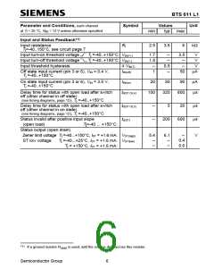
Parameter and Conditions, each channel
Symbol
Values
Unit
at Tj = 25 °C, V = 12 V unless otherwise specified
bb
min
2.5
typ
max
6
Input and Status Feedback11)
Input resistance
Tj=-40..150°C, see circuit page 7
RI
3.5
kΩ
Input turn-on threshold voltage
Input turn-off threshold voltage
Input threshold hysteresis
Tj =-40..+150°C: VIN(T+)
Tj =-40..+150°C: VIN(T-)
∆ VIN(T)
1.7
1.5
--
--
--
3.5
--
V
V
0.5
--
--
V
Off state input current (pin 3 or 6), VIN = 0.4 V,
Tj =-40..+150°C
IIN(off)
1
50
µA
On state input current (pin 3 or 6), VIN = 3.5 V,
Tj =-40..+150°C
IIN(on)
20
50
90
µA
µs
Delay time for status with open load after switch
off (other channel in off state)
(see timing diagrams, page 12), Tj =-40..+150°C
td(ST OL4)
100
320
800
Delay time for status with open load after switch
off (other channel in on state)
td(ST OL5)
--
--
5
20
µs
µs
(see timing diagrams, page 12), Tj =-40..+150°C
Status invalid after positive input slope
td(ST)
200
600
(open load)
T =-40 ... +150°C:
j
Status output (open drain)
Zener limit voltage T =-40...+150°C, IST = +1.6 mA: VST(high)
5.4
--
--
6.1
--
--
--
0.4
0.6
V
j
ST low voltage
T =-40...+25°C, IST = +1.6 mA: VST(low)
j
T = +150°C, IST = +1.6 mA:
j
11)
If a ground resistor R
is used, add the voltage drop across this resistor.
GND
Semiconductor Group
6

 INFINEON [ Infineon ]