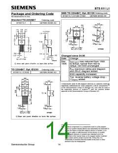
BTS 611 L1
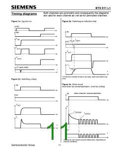
Both channels are symmetric and consequently the diagrams
are valid for each channel as well as for permuted channels
Timing diagrams
Figure 1a: V turn on:
Figure 2b: Switching an inductive load
bb
IN1
IN2
IN
V
bb
td(ST)
ST
*)
V
OUT1
V
OUT
V
OUT2
I L
ST open drain
IL(OL)
t
t
*) if the time constant of load is too large, open-load-status may
occur
Figure 2a: Switching a lamp:
Figure 3a: Short circuit
shut down by overtempertature, reset by cooling
IN
other channel: normal operation
IN
ST
VOUT
IL
I
L(SCp)
I
L(SCr)
IL
t
ST
t
Heating up may require several milliseconds, depending on
external conditions
Semiconductor Group
11

 INFINEON [ Infineon ]