BTS 611 L1
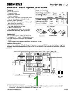
Pin
1
Symbol
OUT1 (Load, L)
GND
Function
Output 1, protected high-side power output of channel 1
Logic ground
2
3
IN1
Input 1, activates channel 1 in case of logical high signal
4
V
Positive power supply voltage,
the tab is shorted to this pin
bb
Diagnostic feedback: open drain, low on failure
5
6
7
ST
IN2
Input 2, activates channel 2 in case of logical high signal
Output 2, protected high-side power output of channel 2
OUT2 (Load, L)
Maximum Ratings at Tj = 25 °C unless otherwise specified
Parameter
Symbol
Values
Unit
V
Supply voltage (overvoltage protection see page 4)
Vbb
Vbb
43
34
Supply voltage for full short circuit protection
Tj Start=-40 ...+150°C
V
4)
Load dump protection2) VLoadDump = UA + Vs, UA = 13.5 V VLoad dump
60
V
RI3)= 2 Ω, RL= 5.3 Ω, td= 200 ms, IN= low or high
Load current (Short circuit current, see page 5)
Operating temperature range
Storage temperature range
IL
self-limited
-40 ...+150
-55 ...+150
A
Tj
Tstg
Ptot
°C
Power dissipation (DC), TC ≤ 25 °C
36
W
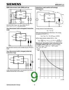
Inductive load switch-off energy dissipation, single pulse
Vbb
=12V, Tj,start =150°C, TC =150°C const.
one channel, IL = 2.3 A, ZL = 89mH, 0 Ω: EAS
290
580
mJ
both channels parallel, IL = 4.4 A, ZL = 47mH, 0 Ω:
see diagrams on page 9
Electrostatic discharge capability (ESD)
(Human Body Model)
IN: VESD
all other pins:
1.0
2.0
kV
acc. MIL-STD883D, method 3015.7 and ESD assn. std. S5.1-1993
Input voltage (DC)
VIN
IIN
IST
-10 ... +16
±2.0
V
mA
Current through input pin (DC)
Current through status pin (DC)
see internal circuit diagrams page 7
±5.0
2)
Supply voltages higher than Vbb(AZ) require an external current limit for the GND and status pins, e.g. with a
150 Ω resistor in the GND connection and a 15 kΩ resistor in series with the status pin. A resistor for the
protection of the input is integrated.
3)
4)
R = internal resistance of the load dump test pulse generator
I
VLoad dump is setup without the DUT connected to the generator per ISO 7637-1 and DIN 40839
Semiconductor Group
2

 INFINEON [ Infineon ]