High Current PN Half Bridge
BTN8982TA
Application Information
6
Application Information
Note:The following information is given as a hint for the implementation of the device only and shall not be
regarded as a description or warranty of a certain functionality, condition or quality of the device.
6.1
Application Circuit
Reverse Polarity
Protection
Microcontroller
Voltage Regulator
(IPD90P03P4L-04)
I/O
Reset
Vdd
WO
TLE
4278G
XC866
RO
Q
I
VS
L1
DZ1
10V
CI
470nF
C
22µF
Q
D
GND
Vss
C1
R
3
CD
47nF
A/D I/O I/O I/O A/D
100nF
10kΩ
optional
R12
10kΩ
R22
10kΩ
BTN8982TA
BTN8982TA
VS
VS
C1O 2V
220nF
C2 O2V
220nF
C
R21
10kΩ
10
R
10kΩ
11
INH
IN
INH
1000µF
OUT
OUT
IN
M
C
100nF
19
IS
IS
C1OUT
C2OUT
C29
R112
1k Ω
R212
1kΩ
220nF
220nF 100nF
SR
SR
C
1nF
1IS
C
1nF
2IS
GND
GND
C12
100nF
R111
0..51kΩ
R
C22
100nF
211
0..51kΩ
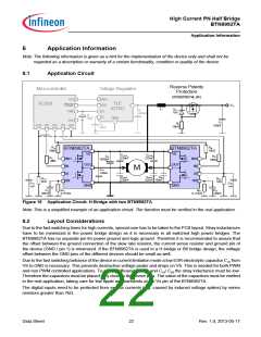
Figure 16 Application Circuit: H-Bridge with two BTN8982TA
Note:This is a simplified example of an application circuit. The function must be verified in the real application.
6.2
Layout Considerations
Due to the fast switching times for high currents, special care has to be taken to the PCB layout. Stray inductances
have to be minimized in the power bridge design as it is necessary in all switched high power bridges. The
BTN8982TA has no separate pin for power ground and logic ground. Therefore it is recommended to assure that
the offset between the ground connection of the slew rate resistor, the current sense resistor and ground pin of
the device (GND / pin 1) is minimized. If the BTN8982TA is used in a H-bridge or B6 bridge design, the voltage
offset between the GND pins of the different devices should be small as well.
Due to the fast switching behavior of the device in current limitation mode a low ESR electrolytic capacitor C10 from
VS to GND is necessary. This prevents destructive voltage peaks and drops on VS. This is needed for both PWM
and non PWM controlled applications. To assure efficiency of C10 and C19/ C29 the stray inductance must be low.
Therefore the capacitors must be placed very close to the device pins. The value of the capacitors must be verified
in the real application, taking care for low ripple and transients at the Vs pin of the BTN8982TA.
The digital inputs need to be protected from excess currents (e.g. caused by induced voltage spikes) by series
resistors greater than 7kΩ.
Data Sheet
22
Rev. 1.0, 2013-05-17

 INFINEON [ Infineon ]