AN985B/BX
Electrical Specifications and Timings
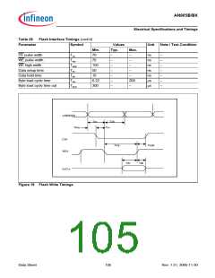
9
Electrical Specifications and Timings
9.1
Absolute Maximum Ratings
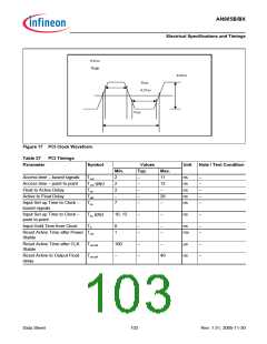
Table 21
Min-Max Ratings
Parameter
Symbol
Values
Typ.
–
–
–
Unit
Note / Test Condition
Min.
-0.5
-0.5
-0.5
- 65
0
Max.
3.6
V
V
150
70
2000
Supply Voltage
Input Voltage
Output Voltage
Storage Temperature
Ambient Temperature
ESD Protection
VCC
VCC
VCC
°C
V
–
CC + 0.5 V
CC + 0.5 V
°C
°C
V
°C
9.2
DC Specifications
Table 22
Parameter
General DC Specifications
Symbol
Values
Unit
Note / Test Condition
Min.
3.0
–
Typ.
–
–
Max.
3.6
1
Supply Voltage
Power Supply
VCC
ICC
V
A
–
–
Table 23
Parameter
PCI Interface DC Specifications
Symbol
Values
Unit
Note / Test Condition
Min.
Typ.
Max.
Input LOW Voltage
Input HIGH Voltage
Input Leakage Current
Output LOW Voltage
Output HIGH Voltage
Input Pin Capacitance
CLK Pin Capacitance
Vilp
Vihp
Iilp
Volp
Vohp
Cinp
Cclkp
-0.5
0.475 VCC
-10
–
0.9 VCC
5
10
–
–
–
–
–
–
–
0.325 VCC
V
–
–
V
CC + 0.5 V
10
0.1 VCC
–
17
22
µA
V
V
pF
pF
0 < Vin < VCC
I
I
out = 700 µA
out = -150 µA
–
–
Table 24
Parameter
Flash/EEPROM Interface DC Specifications
Symbol
Values
Typ.
Unit
Note / Test Condition
Min.
Max.
Input LOW Voltage
Input HIGH Voltage
Input Leakage Current
Output LOW Voltage
Vilf
Vihf
Iif
0
–
–
–
–
0.3 VCC
V
V
µA
V
–
–
–
–
0.7 VCC
?
–
V
CC + 1
?
0.2
Volf
Data Sheet
101
Rev. 1.51, 2005-11-30

 INFINEON [ Infineon ]