AN985B/BX
Electrical Specifications and Timings
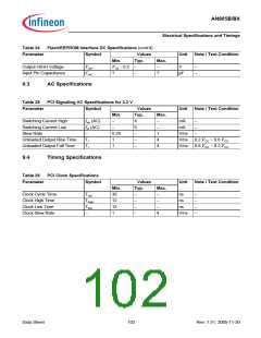
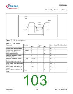
0.6vcc
Thigh
0.4Vcc
Tlow
0.2Vcc
Tcyc
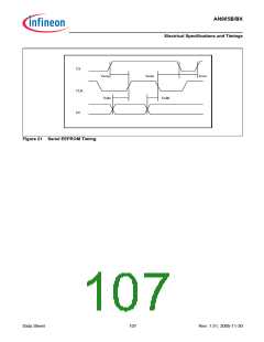
Figure 17 PCI Clock Waveform
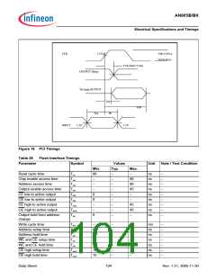
Table 27
PCI Timings
Parameter
Symbol
Values
Typ.
–
–
–
–
–
Unit
Note / Test Condition
Min.
Max.
11
12
–
28
–
Access time – bused signals
Access time – point to point
Float to Active Delay
Active to Float Delay
Input Set up Time to Clock –
bused signals
Tval
2
2
2
–
7
ns
ns
ns
ns
ns
–
–
–
–
–
T
val (ptp)
Ton
Toff
Tsu
Input Set up Time to Clock –
point to point
T
su (ptp)
10, 12
–
–
ns
–
Input Hold Time from Clock
Reset Active Time after Power Trst
Stable
Th
0
1
–
–
–
–
ns
ms
–
–
Reset Active Time after CLK
Stable
Reset Active to Output Float
delay
Trst-clk
100
–
–
–
–
µs
–
–
Trst-off
40
ns
Data Sheet
103
Rev. 1.51, 2005-11-30

 INFINEON [ Infineon ]