IDT72T7285/72T7295/72T72105/72T72115 2.5V TeraSync
16,384 x 72, 32,768 x 72, 65,536 x 72, 131,072 x 72
72-BIT FIFO
COMMERCIAL AND INDUSTRIAL
TEMPERATURE RANGES
t
CLK
t
CLKH
t
CLKL
NO WRITE
NO WRITE
WCLK
2
1
(1)
1
(1)
2
t
SKEW1
t
DH
t
SKEW1
tDS
t
DH
tDS
DX+1
DX
D0 - Dn
tWFF
tWFF
tWFF
tWFF
FF
WEN
RCLK
tENS
tENS
t
ENH
tENH
REN
RCS
tENS
tA
tA
Q0
- Qn
NEXT DATA READ
DATA READ
5994 drw16
tRCSLZ
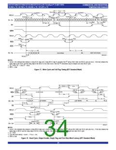
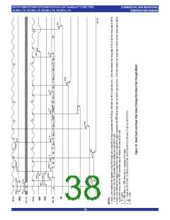
NOTES:
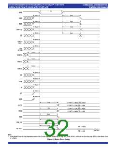
1. tSKEW1 is the minimum time between a rising RCLK edge and a rising WCLK edge to guarantee that FF will go HIGH (after one WCLK cycle pus tWFF). If the time between the
rising edge of the RCLK and the rising edge of the WCLK is less than tSKEW1, then the FF deassertion may be delayed one extra WCLK cycle.
2. LD = HIGH, OE = LOW, EF = HIGH.
3. WCS = LOW.
Figure 11. Write Cycle and Full Flag Timing (IDT Standard Mode)
tCLK
tCLKH
tCLKL
1
2
RCLK
REN
tENH
tENS
tENS
tENH
tENH
tENS
NO OPERATION
NO OPERATION
tREF
tREF
tREF
EF
tA
tA
tA
D0
LAST WORD
D1
LAST WORD
Q0 - Qn
tOLZ
tOHZ
t
OLZ
tOE
OE
WCLK
WEN
t
SKEW1(1)
tENS
tENH
tENH
tENS
tWCSS
tWCSH
WCS
tDS
tDH
tDH
tDS
D0
D1
D0 - Dn
5994 drw17
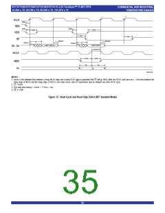
NOTES:
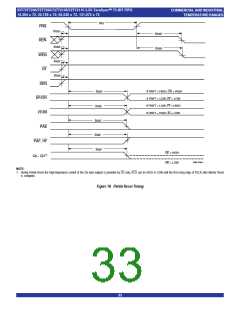
1. tSKEW1 is the minimum time between a rising WCLK edge and a rising RCLK edge to guarantee that EF will go HIGH (after one RCLK cycle plus tREF). If the time between the
rising edge of WCLK and the rising edge of RCLK is less than tSKEW1, then EF deassertion may be delayed one extra RCLK cycle.
2. LD = HIGH.
3. First data word latency = tSKEW1 + 1*TRCLK + tREF.
4. RCS is LOW.
Figure 12. Read Cycle, Output Enable, Empty Flag and First Data Word Latency (IDT Standard Mode)
34

 IDT [ INTEGRATED DEVICE TECHNOLOGY ]