932SQ420D
PCIE GEN 2/3 & QPI CLOCK FOR ROMLEY-BASED SERVERS
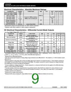
Electrical Characteristics - Absolute Maximum Ratings
PARAMETER
SYMBOL
VDDA
VDD
CONDITIONS
MIN
TYP
MAX
4.6
4.6
UNITS NOTES
3.3V Core Supply Voltage
3.3V Logic Supply Voltage
Input Low Voltage
V
V
V
1,2
1,2
1
VIL
GND-0.5
Input High Voltage
Input High Voltage
VIH
Except for SMBus interface
SMBus clock and data pins
VDD+0.5V
5.5V
V
1
1
VIHSMB
V
°C
°C
°C
V
1
1
1
1
Storage Temperature
Junction Temperature
Case Temperature
Ts
Tj
Tc
-65
150
125
110
Input ESD protection
ESD prot
Human Body Model
2000
1Guaranteed by design and characterization, not 100% tested in production.
2 Operation under these conditions is neither implied nor guaranteed.
DC Electrical Characteristics - Differential Current Mode Outputs
TA = TCOM ; Supply Voltage VDD = 3.3 V +/-5%
PARAMETER
Slew rate
SYMBOL
dV/dt
CONDITIONS
MIN
1
TYP
2.4
MAX
4
UNITS NOTES
Scope averaging on
Slew rate matching, Scope
averaging on
Rise/fall matching, Scope
averaging off
Statistical measurement on
single-ended signal using
oscilloscope math function.
(Scope averaging on)
Measurement on single ended
signal using absolute value.
Scope averaging off
Scope averaging off
Scope averaging off
1, 2, 3
1, 2, 4
V/ns
%
ΔdV/dt
Slew rate matching
Rise/Fall Time Matching
Voltage High
9
20
ps
Trf
Δ
125
850
1, 8, 9
VHigh
VLow
660
772
9
1
1
mV
mV
Voltage Low
-150
150
Max Voltage
Min Voltage
Vswing
Crossing Voltage (abs)
Crossing Voltage (var)
Vmax
Vmin
Vswing
810
-17
1446
351
24
1150
1, 7
1, 7
1, 2
1, 5
1, 6
-300
300
250
mV
mV
mV
Vcross_abs
550
140
-Vcross
Δ
1Guaranteed by design and characterization, not 100% tested in production. IREF = VDD/(3xR ). For R = 475 (1%), I
=
Ω
R
R
REF
2.32mA. IOH = 6 x IREF and VOH = 0.7V @ Z =50 (100 differential impedance).
Ω
Ω
O
2 Measured from differential waveform
3 Slew rate is measured through the Vswing voltage range centered around differential 0V. This results in a +/-150mV window around
differential 0V.
4 Matching applies to rising edge rate for Clock and falling edge rate for Clock#. It is measured using a +/-75mV window centered on
the average cross point where Clock rising meets Clock# falling. The median cross point is used to calculate the voltage thresholds
the oscilloscope is to use for the edge rate calculations.
5 Vcross is defined as voltage where Clock = Clock# measured on a component test board and only applies to the differential rising
edge (i.e. Clock rising and Clock# falling).
6 The total variation of all Vcross measurements in any particular system. Note that this is a subset of V_cross_min/max (V_cross
absolute) allowed. The intent is to limit Vcross induced modulation by setting V_cross_delta to be smaller than V_cross absolute.
7 Includes overshoot and undershoot.
8 Measured from single-ended waveform
9 Measured with scope averaging off, using statistics function. Variation is difference between min and max.
IDT® PCIE GEN 2/3 & QPI CLOCK FOR ROMLEY-BASED SERVERS
9
932SQ420D
REV H 042012

 IDT [ INTEGRATED DEVICE TECHNOLOGY ]