932SQ420D
PCIE GEN 2/3 & QPI CLOCK FOR ROMLEY-BASED SERVERS
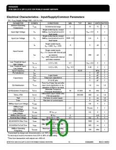
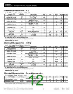
Electrical Characteristics - PCI
TA = 0 - 70°C; Supply Voltage VDD/VDDA = 3.3 V +/-5%,
PARAMETER
Output Impedance
Output High Voltage
Output Low Voltage
SYMBOL
RDSP
CONDITIONS
VO = VDD*(0.5)
MIN
12
TYP
MAX
55
UNITS NOTES
Ω
1
1
1
1
1
1
1
VOH
VOL
IOH = -1 mA
IOL = 1 mA
2.4
V
V
0.55
-33
38
MIN @VOH = 1.0 V
MAX @VOH = 3.135 V
MIN @VOL = 1.95 V
MAX @ VOL = 0.4 V
-33
30
mA
mA
mA
mA
IOH
IOL
Output High Current
Output Low Current
1
1
ns
Clock High Time
THIGH
1.5V
12
Clock Low Time
Edge Rate
TLOW
tslewr/f
dt1
1.5V
12
1
45
ns
V/ns
%
ps
ps
Rising/Falling edge rate
VT = 1.5 V
1.8
50.5
294
108
4
55
1,2
1
1
Duty Cycle
Group Skew
tskew
tjcyc-cyc
VT = 1.5 V
VT = 1.5 V
500
500
Jitter, Cycle to cycle
1
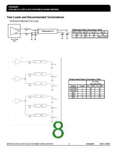
See "Single-ended Test Loads Page" for termination circuits
1Guaranteed by design and characterization, not 100% tested in production.
2 Measured between 0.8V and 2.0V
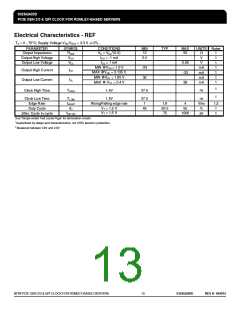
Electrical Characteristics - 48MHz
TA = 0 - 70°C; Supply Voltage VDD/VDDA = 3.3 V +/-5%,
PARAMETER
Output Impedance
Output High Voltage
Output Low Voltage
SYMBOL
RDSP
CONDITIONS
VO = VDD*(0.5)
MIN
20
TYP
MAX
60
UNITS NOTES
Ω
1
1
1
1
1
1
1
VOH
VOL
IOH = -1 mA
IOL = 1 mA
2.4
V
V
0.55
-33
MIN @VOH = 1.0 V
MAX @VOH = 3.135 V
MIN @VOL = 1.95 V
MAX @ VOL = 0.4 V
-29
29
mA
mA
mA
mA
IOH
IOL
Output High Current
Output Low Current
Clock High Time
27
1
1
ns
THIGH
1.5V
1.5V
8.094
10.036
Clock Low Time
Edge Rate
TLOW
tslewr/f_USB
7.694
1
45
9.836
2
55
ns
V/ns
%
Rising/Falling edge rate
VT = 1.5 V
1.5
51
1,2
1
Duty Cycle
dt1
tjcyc-cyc
VT = 1.5 V
109
350
ps
Jitter, Cycle to cycle
1
See "Single-ended Test Loads Page" for termination circuits
1Guaranteed by design and characterization, not 100% tested in production.
2 Measured between 0.8V and 2.0V
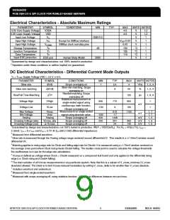
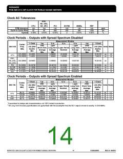
Electrical Characteristics - Current Consumption
TA = TCOM; Supply Voltage VDD = 3.3 V +/-5%
PARAMETER
Operating Supply Current
Powerdown Current
SYMBOL
IDD3.3OP
CONDITIONS
MIN
TYP
MAX
UNITS NOTES
All outputs active @100MHz, CL
380
16
400
20
mA
mA
1
1
= Full load;
All differential pairs tri-stated
IDD3.3PDZ
1Guaranteed by design and characterization, not 100% tested in production.
IDT® PCIE GEN 2/3 & QPI CLOCK FOR ROMLEY-BASED SERVERS
12
932SQ420D
REV H 042012

 IDT [ INTEGRATED DEVICE TECHNOLOGY ]