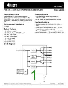
932SQ420D
PCIE GEN 2/3 & QPI CLOCK FOR ROMLEY-BASED SERVERS
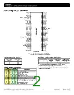
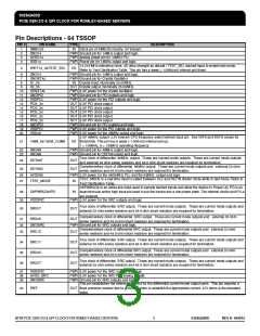
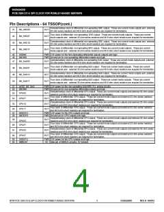
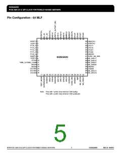
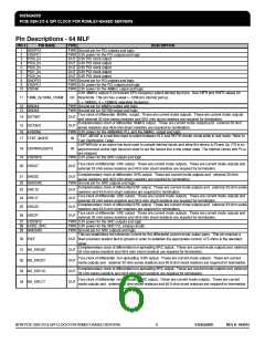
Pin Descriptions - 64 TSSOP
PIN #
PIN NAME
TYPE
DESCRIPTION
1
2
3
4
SMBCLK
IN Clock pin of SMBUS circuitry, 5V tolerant
GND14
AVDD14
VDD14
PWR Ground pin for 14MHz output and logic.
PWR Analog power pin for 14MHz PLL
PWR Power pin for 14MHz output and logic
14.318 MHz reference clock. 3X drive strength as default / TEST_SEL latched input to enable test mode.
Refer to Test Clarification Table. This pin has a weak (~120Kohm) internal pull down.
5
vREF14_3x/TEST_SEL
I/O
6
7
8
9
GND14
GNDXTAL
X1_25
PWR Ground pin for 14MHz output and logic.
PWR Ground pin for Crystal Oscillator.
IN Crystal input, Nominally 25.00MHz.
OUT Crystal output, Nominally 25.00MHz.
PWR 3.3V power for the crystal oscillator.
PWR Ground pin for PCI outputs and logic.
PWR 3.3V power for the PCI outputs and logic
OUT 3.3V PCI clock output
OUT 3.3V PCI clock output
OUT 3.3V PCI clock output
OUT 3.3V PCI clock output
OUT 3.3V PCI clock output
X2_25
10
11
12
13
14
15
16
17
18
19
20
VDDXTAL
GNDPCI
VDDPCI
PCI4_2x
PCI3_2x
PCI2_2x
PCI1_2x
PCI0_2x
GNDPCI
VDDPCI
VDD48
PWR Ground pin for PCI outputs and logic.
PWR 3.3V power for the PCI outputs and logic
PWR 3.3V power for the 48MHz output and logic
3.3V 48MHz output/ 3.3V tolerant CPU frequency select latched input pin. See VilFS and VihFS values for
21
^48M_2x/100M_133M#
I/O thresholds. This pin has a weak (~120Kom) internal pull up.
1 = 100MHz, 0 = 133MHz operating frequency
22
23
GND48
GND96
PWR Ground pin for 48MHz output and logic.
PWR Ground pin for DOT96 output and logic.
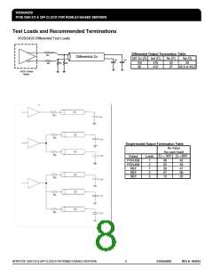
True clock of differential 96MHz output. These are current mode outputs. These are current mode outputs
and external 33 ohm series resistors and 49.9 ohm shunt resistors are required for termination.
24
DOT96T
OUT
Complementary clock of differential 96MHz output. These are current mode outputs and external 33 ohm
series resistors and 49.9 ohm shunt resistors are required for termination.
PWR 3.3V power for the 48/96MHz PLL and the 96MHz output and logic
25
26
27
DOT96C
OUT
AVDD96
TEST_MODE is a real time input to select between Hi-Z and REF/N divider mode while in test mode. Refer to
Test Clarification Table.
TEST_MODE
IN
CKPWRGD# is an active low input used to sample latched inputs and allow the device to Power Up. PD is an
28
29
30
CKPWRGD#/PD
VDDSRC
IN asynchronous active high input pin used to put the device into a low power state. The internal clocks and PLLs
are stopped.
PWR 3.3V power for the SRC outputs and logic
True clock of differential SRC output. These are current mode outputs. These are current mode outputs and
external 33 ohm series resistors and 49.9 ohm shunt resistors are required for termination.
SRC0T
OUT
Complementary clock of differential SRC output. These are current mode outputs and external 33 ohm
series resistors and 49.9 ohm shunt resistors are required for termination.
PWR Ground pin for SRC outputs and logic.
31
32
33
SRC0C
GNDSRC
SRC1C
OUT
Complementary clock of differential SRC output. These are current mode outputs and external 33 ohm
series resistors and 49.9 ohm shunt resistors are required for termination.
OUT
True clock of differential SRC output. These are current mode outputs. These are current mode outputs and
external 33 ohm series resistors and 49.9 ohm shunt resistors are required for termination.
34
35
36
SRC1T
SRC2C
SRC2T
OUT
Complementary clock of differential SRC output. These are current mode outputs and external 33 ohm
series resistors and 49.9 ohm shunt resistors are required for termination.
OUT
True clock of differential SRC output. These are current mode outputs. These are current mode outputs and
external 33 ohm series resistors and 49.9 ohm shunt resistors are required for termination.
OUT
37
38
39
VDDSRC
AVDD_SRC
GNDSRC
PWR 3.3V power for the SRC outputs and logic
PWR 3.3V power for the SRC PLL analog circuits
PWR Ground pin for SRC outputs and logic.
This pin establishes the reference current for the differential current-mode output pairs. This pin requires a
40
IREF
OUT fixed precision resistor tied to ground in order to establish the appropriate current. 475 ohms is the standard
value.
IDT® PCIE GEN 2/3 & QPI CLOCK FOR ROMLEY-BASED SERVERS
3
932SQ420D
REV H 042012

 IDT [ INTEGRATED DEVICE TECHNOLOGY ]