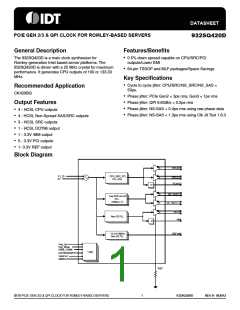
932SQ420D
PCIE GEN 2/3 & QPI CLOCK FOR ROMLEY-BASED SERVERS
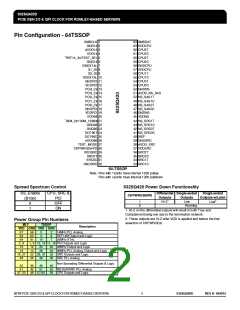
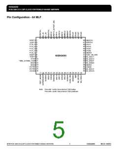
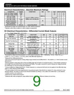
Pin Configuration - 64TSSOP
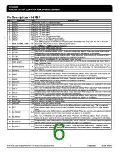
SMBCLK 1
GND14 2
AVDD14 3
VDD14 4
64 SMBDAT
63 VDDCPU
62 CPU3T
61 CPU3C
60 CPU2T
59 CPU2C
vREF14_3x/TEST_SEL 5
GND14 6
GNDXTAL 7
X1_25 8
58 GNDCPU
57 VDDCPU
56 CPU1T
X2_25 9
VDDXTAL 10
GNDPCI 11
VDDPCI 12
PCI4_2x 13
PCI3_2x 14
PCI2_2x 15
PCI1_2x 16
PCI0_2x 17
GNDPCI 18
VDDPCI 19
VDD48 20
55 CPU1C
54 CPU0T
53 CPU0C
52 GNDNS
51 AVDD_NS_SAS
50 NS_SAS1T
49 NS_SAS1C
48 NS_SAS0T
47 NS_SAS0C
46 GNDNS
45 VDDNS
^48M_2x/100M_133M# 21
GND48 22
44 NS_SRC1T
43 NS_SRC1C
42 NS_SRC0T
41 NS_SRC0C
40 IREF
GND96 23
DOT96T 24
DOT96C 25
AVDD96 26
39 GNDSRC
38 AVDD_SRC
37 VDDSRC
36 SRC2T
TEST_MODE 27
CKPWRGD#/PD 28
VDDSRC 29
SRC0T 30
35 SRC2C
SRC0C 31
34 SRC1T
GNDSRC 32
33 SRC1C
64-TSSOP
Note: Pins with ^ prefix have internal 120K pullup
Pins with v prefix have internal 120K pulldown
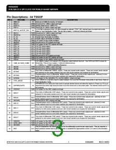
Spread Spectrum Control
932SQ420 Power Down Functionality
SS_Enable
(B1b0)
CPU, SRC &
Differential Single-ended
Single ended
CKPWRGD#/PD
Outputs
Outputs
Low
Outputs w/Latch
PCI
OFF
ON
Low2
1
0
HI-Z1
0
1
Running
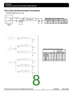
1. Hi-Z on the differential outputs will result in both True and
Complement being low due to the termination network
2. These outputs are Hi-Z after VDD is applied and before the first
assertion of CKPWRGD#.
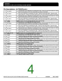
Power Group Pin Numbers
MLF
TSSOP
Description
VDD GND VDD GND
57
58
64
56
60
61
3
4
10
2
6
7
14MHz PLL Analog
REF14M Output and Logic
25MHz XTAL
2, 9
10
16
19, 27
28
1, 8 12, 19 11, 18 PCI Outputs and Logic
12
13
20
26
22 48MHz Output and Logic
23 96MHz PLL Analog, Output and Logic
32 SRC Outputs and Logic
39 SRC PLL Analog
22 29, 37
29
38
Non-Spreading Differential Outputs & Logic
46
52 NS-SAS/SRC PLL Analog
58 CPU Outputs and Logic
35
41
47, 53
36
42
45
51
48 57,63
IDT® PCIE GEN 2/3 & QPI CLOCK FOR ROMLEY-BASED SERVERS
2
932SQ420D
REV H 042012

 IDT [ INTEGRATED DEVICE TECHNOLOGY ]