ICS853P022
UAL LVCMOS / LVTTL-TO-DIFFERENTIAL
3.3V LVPECL TRANSLATOR
Integrated
Circuit
Systems, Inc.
D
GENERAL DESCRIPTION
FEATURES
The ICS853P022 is a Dual LVCMOS / LVTTL-to- • 2 differential 3.3V LVPECL outputs
ICS
Differential 3.3V LVPECL translator and a mem-
• LVCMOS/LVTTL clock inputs
HiPerClockS™
ber of the HiPerClocks™ family of High Perfor-
mance Clocks Solutions from ICS. The
ICS853P022 has single ended clock inputs.The
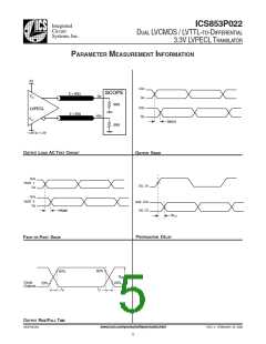
• Maximum output frequency: 1.1GHz
• Part-to-part skew: 650ps (maximum)
• Propagation Delay: 320ps (typical)
• Additive phase jitter, RMS: 0.03ps (typical)
single ended clock input accepts LVCMOS or LVTTL input
levels and translate them to LVPECL levels.The small outline
8-pin TSSOP package makes this device ideal for applica-
tions where space, high performance and low power are im-
portant.
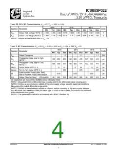
• LVPECL mode operating voltage supply range:
VCC = 3.0V to 3.8V, VEE = 0V
• ECL mode operating voltage supply range:
VCC = 0V, VEE = -3.8V to -3.0V
• -40°C to 85°C ambient operating temperature
• Lead-Free package RoHS compliant
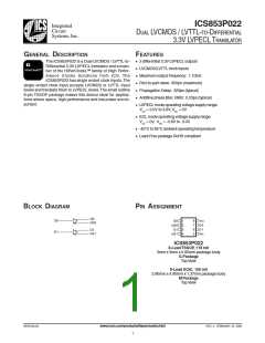
BLOCK DIAGRAM
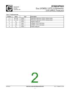
PIN ASSIGNMENT
Q0
nQ0
D0
Q0
nQ0
Q1
VCC
D0
D1
VEE
1
2
3
4
8
7
6
5
Q1
nQ1
D1
nQ1
ICS853P022
8-LeadTSSOP, 118 mil
3mm x 3mm x 0.95mm package body
G Package
TopView
8-Lead SOIC, 150 mil
3.90mm x 4.90mm x 1.37mm package body
M Package
TopView
853P022AG
www.icst.com/products/hiperclocks.html
REV. A FEBRUARY 23, 2005
1

 IDT [ INTEGRATED DEVICE TECHNOLOGY ]