ICS853P022
UAL LVCMOS / LVTTL-TO-DIFFERENTIAL
3.3V LVPECL TRANSLATOR
Integrated
Circuit
Systems, Inc.
D
POWER CONSIDERATIONS
This section provides information on power dissipation and junction temperature for the ICS853P022.
Equations and example calculations are also provided.
1. Power Dissipation.
The total power dissipation for the ICS853P022 is the sum of the core power plus the power dissipated in the load(s).
The following is the power dissipation for VCC = 3.8V, which gives worst case results.
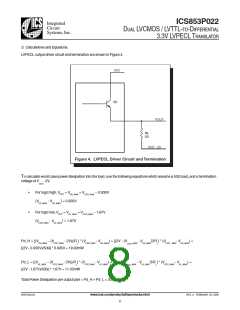
NOTE: Please refer to Section 3 for details on calculating power dissipated in the load.
•
•
Power (core)MAX = VCC_MAX * IEE_MAX = 3.8V * 35mA = 133mW
Power (outputs)MAX = 30.94mW/Loaded Output pair
If all outputs are loaded, the total power is 2 * 30.94mW = 61.88mW
Total Power_MAX (3.8V, with all outputs switching) = 133mW + 61.88mW = 194.88mW
2. Junction Temperature.
Junction temperature, Tj, is the temperature at the junction of the bond wire and bond pad and directly affects the reliability of the
device.The maximum recommended junction temperature for HiPerClockSTM devices is 125°C.
The equation for Tj is as follows: Tj = θJA * Pd_total + TA
Tj = JunctionTemperature
θJA = Junction-to-AmbientThermal Resistance
Pd_total =Total Device Power Dissipation (example calculation is in section 1 above)
TA = AmbientTemperature
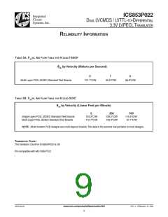
In order to calculate junction temperature, the appropriate junction-to-ambient thermal resistance θJA must be used. Assuming a
moderate air flow of 1 meters per second and a multi-layer board, the appropriate value is 90.5°C/W perTable 4A below.
Therefore, Tj for an ambient temperature of 85°C with all outputs switching is:
85°C + 0.195W * 90.5°C/W = 102.6°C. This is below the limit of 125°C.
This calculation is only an example.Tj will obviously vary depending on the number of loaded outputs, supply voltage, air flow,
and the type of board (single layer or multi-layer).
TABLE 4A. THERMAL RESISTANCE θJA FOR 8-PIN TSSOP, FORCED CONVECTION
θJA byVelocity (Meters per Second)
0
1
2
Multi-Layer PCB, JEDEC StandardTest Boards
101.7°C/W
90.5°C/W
89.8°C/W
TABLE 4B. THERMAL RESISTANCE θJA FOR 8 LEAD SOIC
θJA byVelocity (Linear Feet per Minute)
0
200
128.5°C/W
103.3°C/W
500
115.5°C/W
97.1°C/W
Single-Layer PCB, JEDEC Standard Test Boards
Multi-Layer PCB, JEDEC Standard Test Boards
153.3°C/W
112.7°C/W
NOTE: Most modern PCB designs use multi-layered boards.The data in the second row pertains to most designs.
853P022AG
www.icst.com/products/hiperclocks.html
REV. A FEBRUARY 23, 2005
7

 IDT [ INTEGRATED DEVICE TECHNOLOGY ]