ICS853P022
UAL LVCMOS / LVTTL-TO-DIFFERENTIAL
3.3V LVPECL TRANSLATOR
Integrated
Circuit
Systems, Inc.
D
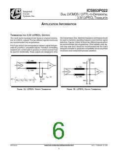
APPLICATION INFORMATION
TERMINATION FOR 3.3V LVPECL OUTPUTS
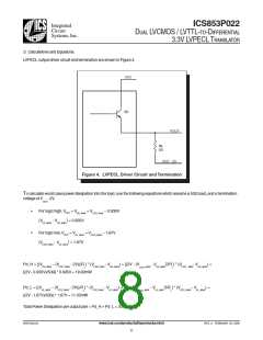
The clock layout topology shown below is a typical termina-
tion for LVPECL outputs.The two different layouts mentioned
are recommended only as guidelines.
50Ω transmission lines. Matched impedance techniques should
be used to maximize operating frequency and minimize signal
distortion. Figures 1A and 1B show two different layouts which
are recommended only as guidelines. Other suitable clock lay-
outs may exist and it would be recommended that the board
designers simulate to guarantee compatibility across all printed
circuit and clock component process variations.
FOUT and nFOUT are low impedance follower outputs that gen-
erate ECL/LVPECL compatible outputs.Therefore, terminating
resistors (DC current path to ground) or current sources must
be used for functionality. These outputs are designed to drive
3.3V
Z
o = 50Ω
125Ω
125Ω
FOUT
FIN
Zo = 50Ω
Zo = 50Ω
Zo = 50Ω
FOUT
FIN
50Ω
50Ω
VCC - 2V
1
RTT =
Zo
RTT
((VOH + VOL) / (VCC – 2)) – 2
84Ω
84Ω
FIGURE 1A. LVPECL OUTPUT TERMINATION
FIGURE 1B. LVPECL OUTPUT TERMINATION
853P022AG
www.icst.com/products/hiperclocks.html
REV. A FEBRUARY 23, 2005
6

 IDT [ INTEGRATED DEVICE TECHNOLOGY ]