ICS853P022
UAL LVCMOS / LVTTL-TO-DIFFERENTIAL
3.3V LVPECL TRANSLATOR
Integrated
Circuit
Systems, Inc.
D
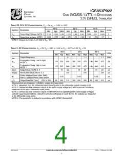
TABLE 2D. ECL DC CHARACTERISTICS, VCC = 0V; VEE = -3.8V TO -3.0V
-40°C
25°C
Typ
85°C
Typ
Symbol Parameter
Units
Min
Typ
Max
Min
Max
Min
Max
-1.125 -1.025 -0.92 -1.075 -1.005 -0.93 -1.005 -0.97 -0.935
-1.895 -1.755 -1.62 -1.875 -1.78 -1.685 -1.86 -1.765 -1.67
VOH
VOL
Output High Voltage; NOTE 1
Output Low Voltage; NOTE 1
V
V
NOTE 1: Outputs terminated with 50Ω to VCC - 2V.
TABLE 3. AC CHARACTERISTICS, VCC = 0V; VEE = -3.8V TO -3.0V OR VCC = 3.0V TO 3.8V; VEE = 0V
-40°C
Min Typ
25°C
Max Min Typ
85°C
Max Min Typ
Symbol Parameter
Units
Max
fMAX
tpLH
Output Frequency
1.1
1.1
1.1
GHz
ps
Propagation Delay, Low to High;
NOTE 1
125 320
600
180 320
475
190 300
410
410
Propagation Delay, High to Low;
NOTE 1
tpHL
125 320
12
600
180 320
12
475
190 300
12
ps
tsk(o)
Output Skew; NOTE 2, 4
55
50
50
ps
ps
tsk(pp)
Part-to-Part Skew; NOTE 3, 4
330
225
225
Buffer Additive Phase Jitter, RMS;
refer to Additive Phase Jitter section
tjit
0.03
0.03
0.03
ps
ps
tR/tF
Output Rise/Fall Time
20% to 80%
85
200
315
100 200
285
85
200
315
All parameters are measured ≤ 650MHz unless otherwise noted.
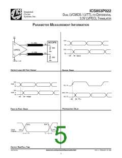
NOTE 1: Measured from the differential input crossing point to the differential output crossing point.
NOTE 2: Defined as skew between outputs at the same supply voltage and with equal load conditions.
Measured at the output differential cross points.
NOTE 3: Defined as skew between outputs on different devices operating at the same supply voltages
and with equal load conditions. Using the same type of inputs on each device, the outputs are measured
at the differential cross points.
NOTE 4: This parameter is defined in accordance with JEDEC Standard 65.
853P022AG
www.icst.com/products/hiperclocks.html
REV. A FEBRUARY 23, 2005
4

 IDT [ INTEGRATED DEVICE TECHNOLOGY ]