ICS1493-19
CLOCK GENERATOR FOR AUTOMOTIVE APPLICATION
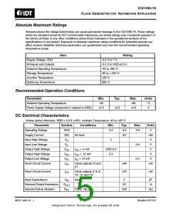
Parameter
Symbol
Conditions
Min.
Typ.
Max.
Units
Internal Pull-down Resistor
R
All clock outputs
except SSEN pin
200
kΩ
Pd
SSEN pin
100
kΩ
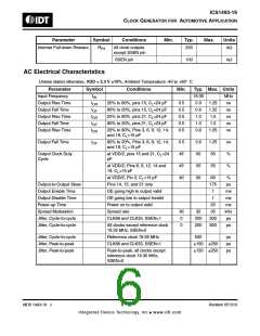
AC Electrical Characteristics
Unless stated otherwise, VDD = 3.3 V 10%, Ambient Temperature -40 to +85° C
Parameter
Input Frequency
Output Rise Time
Output Fall Time
Output Rise Time
Output Fall Time
Output Rise Time
Symbol
Conditions
Min.
Typ. Max. Units
f
19.35
0.9
MHz
ns
IN
t
20% to 80%, pins 15, C =24 pF
0.5
0.5
0.5
0.5
0.5
1.25
1.25
1.5
OR
L
t
80% to 20%, pins 15, C =24 pF
0.9
ns
OF
OR
L
t
20% to 80%, pins 21, C =24 pF
1.0
ns
L
t
80% to 20%, pins 21, C =24 pF
1.0
1.5
ns
OF
OR
L
t
20% to 80%, Pins 3, 6, 9, 12, 14,
0.9
1.25
ns
and 19, C =15 pF
L
Output Fall Time
t
80% to 20%, Pins 3, 6, 9, 12, 14,
0.5
45
45
40
0.9
50
50
50
1.25
55
ns
%
%
OF
and 19, C =15 pF
L
Output Clock Duty
Cycle
at VDD/2, pins 15 and 21, C =24
L
pF
at VDD/2, Pins 6, 9, 12, 14 and
55
19, C =15 pF
L
at VDD/2, Pin 3, C =15 pF
60
175
1
%
ps
L
Output-to-Output Skew
Output Enable Time
Output Disable Time
Power-up Time
Pins 14, 15, and 21 only
OE going high to output valid
OE going low to output Invalid
Power on to output valid
Spread rate
ms
ms
ms
kHz
ps
1
20
35
300
300
Spread Modulation
Jitter, Cycle-to-cycle
Jitter, Cycle-to-cycle
30
0
32
CLK66 and CLK33, SSEN=1
200
200
All clocks except reference clock
19.35 MHz, SSEN=0
0
ps
Jitter, Cycle-to-cycle
Jitter, Peak-to-peak
Jitter, Peak-to-peak
Reference clock 19.35 MHz
CLK66 and CLK33, SSEN=1
500
150
150
ps
ps
ps
250
250
Peak-to-peak, all clocks except
reference clock 19.35 MHz,
SSEN=0
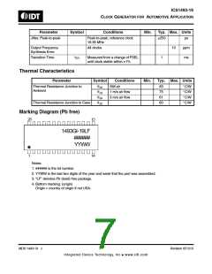
MDS 1493-19 J
6
Revision 051310
Integrated Device Technology, Inc.● www.idt.com

 IDT [ INTEGRATED DEVICE TECHNOLOGY ]