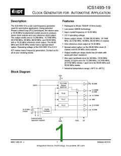
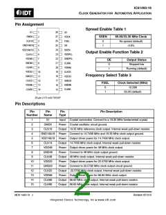
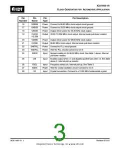
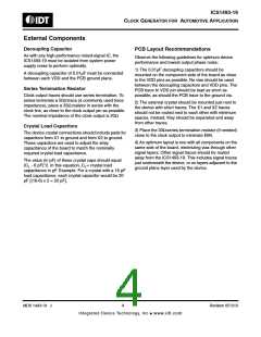
ICS1493-19
CLOCK GENERATOR FOR AUTOMOTIVE APPLICATION
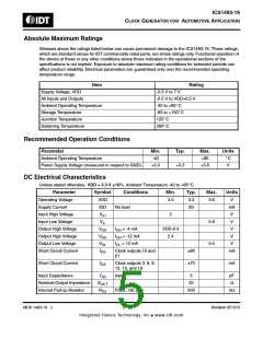
Absolute Maximum Ratings
Stresses above the ratings listed below can cause permanent damage to the ICS1493-19. These ratings,
which are standard values for IDT commercially rated parts, are stress ratings only. Functional operation of
the device at these or any other conditions above those indicated in the operational sections of the
specifications is not implied. Exposure to absolute maximum rating conditions for extended periods can
affect product reliability. Electrical parameters are guaranteed only over the recommended operating
temperature range.
Item
Rating
Supply Voltage, VDD
All Inputs and Outputs
-0.5 V to 7 V
-0.5 V to VDD+0.5 V
-40 to +85° C
-65 to +150° C
125°C
Ambient Operating Temperature
Storage Temperature
Junction Temperature
Soldering Temperature
260°C
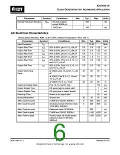
Recommended Operation Conditions
Parameter
Min.
Typ.
Max.
+85
Units
° C
Ambient Operating Temperature
Power Supply Voltage (measured in respect to GND)
-40
+3.0
+3.3
+3.6
V
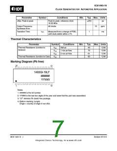
DC Electrical Characteristics
Unless stated otherwise, VDD = 3.3 V 10%, Ambient Temperature -40 to +85°C
Parameter
Operating Voltage
Supply Current
Symbol
VDD
Conditions
Min.
Typ.
3.3
Max.
Units
3.0
3.6
0.8
0.4
V
mA
V
IDD
No load
80
Input High Voltage
Input Low Voltage
Output High Voltage
Output High Voltage
Output Low Voltage
Short Circuit Current
V
2
IH
V
V
IL
V
V
I
I
I
= -4 mA
= -12 mA
= 12 mA
VDD-0.4
2.4
V
OH
OH
OH
OH
OL
V
V
V
OL
OS
I
Clock outputs,15 and
21
80
70
mA
Short Circuit Current
I
Clock outputs 3, 6, 9,
12, 14, and 19
mA
OS
Input Capacitance
C
Input
5
pF
Ω
IN
Nominal Output Impedance
Internal Pull-up Resistor
Z
20
OUT
R
FSEL, OE pins
200
kΩ
PU
MDS 1493-19 J
5
Revision 051310
Integrated Device Technology, Inc.● www.idt.com

 IDT [ INTEGRATED DEVICE TECHNOLOGY ]