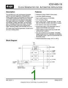
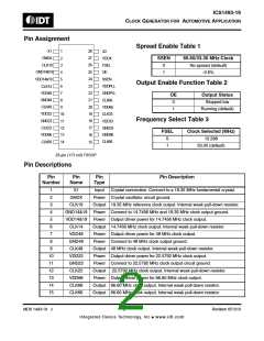
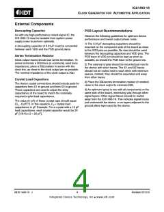
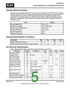
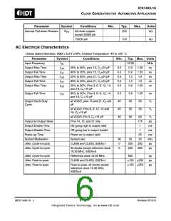
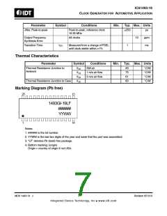
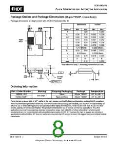
ICS1493-19
CLOCK GENERATOR FOR AUTOMOTIVE APPLICATION
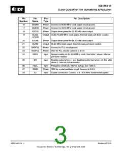
Pin
Number
Pin
Name
Pin
Type
Pin Description
16
17
18
19
GND66
GND33
VDD33
Power Connect to 66.60 MHz clock output circuit ground.
Power Connect to 33.30 MHz clock output circuit ground.
Power Output driver power for 33.30 MHz clock output.
Output 33.30 /12.288 MHz clock output. Internal weak pull-down resistor.
CLK33
/12.288
20
21
22
23
24
VDD66
CLK66
Power Output driver power for 66.60 MHz clock output.
Output 66.60 MHz clock output. Internal weak pull-down resistor.
Power Connect to PLL circuit ground.
GNDPLL
VDDPLL
SSEN
Power VDD for PLL circuits Connect to 3.3 V.
Input
Input
Input
Spread enable pin for 66.60 MHz clock. See table 1 above. Internal
pull-down resistor.
25
OE
Enables output when =1 and disables (pulled low) when =0. See table
above 2. Internal pull-up resistor.
26
27
28
FSEL
VDDX
X2
Frequency select pin, internal pull-up. See Table 3.
Power VDD for crystal oscillator circuit. Connect to 3.3.V.
Input Crystal connection. Connect to a 19.35 MHz fundamental crystal.
MDS 1493-19 J
3
Revision 051310
Integrated Device Technology, Inc.● www.idt.com

 IDT [ INTEGRATED DEVICE TECHNOLOGY ]