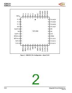
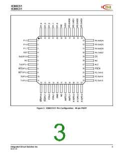
IC80C51
IC80C31
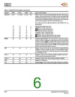
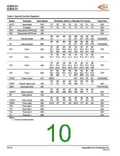
Table 1. Detailed Pin Description (continued)
Symbol
PDIP
PLCC
PQFP I/O
Name and Function
P3.0-P3.7
10-17
11, 13-19
5, 7-13 I/O
Port 3: Port 3 is an 8-bit bidirectional I/O port with internal
pullups. Port 3 pins that have 1s written to them are pulled high
by the internal pullups and can be used as inputs. As inputs, Port
3 pins that are externally pulled low will source current because
of the internal pullups. (See DC Characteristics: IIL).
Port 3 also serves the special features of the IC80C51/31, as
listed below:
10
11
12
13
14
15
16
17
11
13
14
15
16
17
18
19
5
7
8
I
O
I
I
I
I
O
O
RxD (P3.0): Serial input port.
TxD (P3.1): Serial output port.
INT0 (P3.2): External interrupt 0.
INT1 (P3.3): External interrupt 1.
T0 (P3.4): Timer 0 external input.
T1 (P3.5): Timer 1 external input.
WR (P3.6): External data memory write strobe.
RD (P3.7): External data memory read strobe.
9
10
11
12
13
PSEN
29
32
26
O
Program Store Enable: The read strobe to external program
memory. When the device is executing code from the external
program memory, PSEN is activated twice each machine cycle
except that two PSEN activations are skipped during each
access to external data memory. PSEN is not activated during
fetches from internal program memory.
RST
9
10
21
4
I
I
Reset: A high on this pin for two machine cycles while the
oscillator is running, resets the device. An internal MOS resistor
to GND permits a power-on reset using only an external capaci-
tor connected to Vcc.
XTAL 1
19
15
Crystal 1: Input to the inverting oscillator amplifier and input
to the internal clock generator circuits.
XTAL 2
GND
Vcc
18
20
40
20
22
44
14
16
38
O
I
Crystal 2: Output from the inverting oscillator amplifier.
Ground: 0V reference.
I
Power Supply: This is the power supply voltage for operation.
S3-6
Integrated Circuit Solution Inc.
MC001-0B

 ICSI [ INTEGRATED CIRCUIT SOLUTION INC ]