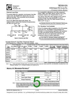
M2006-02A
Integrated
Circuit
Systems, Inc.
VCSO BASED FEC CLOCK PLL
P r o d u c t D a t a S h e e t
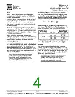
PLL bandwidth is affected by loop filter component
values, “Mfec” and “Mfin” values, and the “PLL Loop
Constants” listed in AC Characteristics on pg. 7.
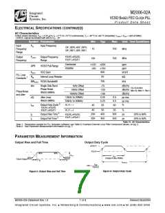
External Loop Filter
To provide stable PLL operation, and thereby a low jitter
output clock, the M2006-02A requires the use of an
external loop filter. This is provided via the provided
filter pins (see Figure 4).
The various “Non-FEC ratio” settings can be used to
actively change PLL loop bandwidth in a given
application. See “FEC PLL Ratio Dividers Look-up
Table (LUT)” on pg. 3.
Due to the differential signal path design, the
implementation requires two identical complementary
RC filters as shown here.
See Example External Loop Filter Component Values table.
RLOOP CLOOP
RPOST
PLL Simulator Tool Available
CPOST
CPOST
A free PC software utility is available on the ICS website
(www.icst.com). The M2000 Timing Modules PLL
Simulator is a downloadable application that simulates
PLL jitter and wander transfer characteristics. This
enables the user to set appropriate external loop
component values in a given application.
RLOOP CLOOP
nOP_IN OP_OUT
RPOST
OP_IN
nOP_OUT
nVC
VC
4
9
8
5
6
7
Go to the SAW PLL Simulator Software web page at
www.icst.com/products/calculators/m2000filterSWdesc.htm
Figure 4: External Loop Filter
1
Example External Loop Filter Component Values
VCSO Parameters: K
= 800kHz/V, R = 50k
Ω
, VCSO Bandwidth = 700kHz.
VCO
IN
Device Configuration
FIN_SEL1:0 FEC_ SEL3:0
Example External Loop Filter Component Values Nominal Performance Using These Values
FRef
F
VCSO (MHz)
R loop
C loop
R post
C post
PLL Loop Damping Passband
pins
pins
Bandwidth
Factor Peaking(dB)
(MHz)
0 0
0 1
1 0
1 1
1 0
1 1
1 0
1 1
1 1 0 0
1 1 1 0
1 1 1 1
0 1 1 0
0 0 0 1
6.0
0.05
19.44
622.08
11.5kΩ
2.2µF
34kΩ
470pF
1kHz
77.76
155.52
622.08
167.3317
669.3266
155.52
622.08
6.0
6.0
6.3
6.0
6.5
0.06
0.06
0.05
0.05
0.05
5.11kΩ
113.0kΩ
28.0kΩ
121.0kΩ
30.1kΩ
4.7µF
0.22µF
1.0µF
0.22µF
1.0µF
1 0 0 1
669.3266
Table 8: Example External Loop Filter Component Values
Note 1: KVCO , VCSO Bandwidth, M Divider Value, and External Loop Filter Component Values determine Loop Bandwidth, Damping Factor, and
Passband Peaking. For PLL Simulator software, go to www.icst.com.
1
ABSOLUTE MAXIMUM RATINGS
Symbol Parameter
Rating
Unit
VI
Inputs
-0.5 to VCC +0.5
V
VO
VCC
TS
Outputs
-0.5 to VCC +0.5
4.6
V
V
Power Supply Voltage
Storage Temperature
-45 to +100
oC
Table 9: Absolute Maximum Ratings
Note 1: Stresses beyond those listed under Absolute Maximum Ratings may cause permanent damage to the
device. These ratings are stress specifications only. Functional operation of product at these conditions
or any conditions beyond those listed in Recommended Conditions of Operation, DC Characteristics, or
AC Characteristics is not implied. Exposure to absolute maximum rating conditions for extended periods
may affect product reliability
.
M2006-02A Datasheet Rev 1.0
5 of 8
Revised 28Jul2004
Integrated Circuit Systems, Inc. ● Networking & Communications ● www.icst.com ● tel (508) 852-5400

 ICSI [ INTEGRATED CIRCUIT SOLUTION INC ]