M2006-02A
Integrated
Circuit
Systems, Inc.
VCSO BASED FEC CLOCK PLL
P r o d u c t D a t a S h e e t
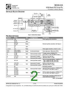
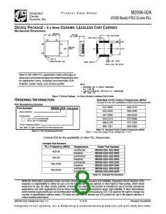
DETAILED BLOCK DIAGRAM
RLOOP CLOOP
RPOST
External
Loop Filter
Components
CPOST
CPOST
RLOOP CLOOP
nOP_IN OP_OUT
RPOST
A
M2006-02
OP_IN
RIN
nOP_OUT
nVC
VC
MUX
Phase
Detector
SAW Delay Line
DIF_REF0
Phase
Locked
Loop
0
Rfec
Divider
nDIF_REF0
RIN
DIF_REF1
nDIF_REF1
Loop Filter
Amplifier
Phase
Shifter
1
(PLL)
VCSO
Mfec Divider
Mfin Divider
REF_SEL
P0 Divider
FOUT0
nFOUT0
P = 1 ( P0_SEL = 0 )
or
4 ( P0_SEL = 1 )
4
2
Mfec / Rfec
Divider LUT
FEC_SEL3:0
FIN_SEL1:0
P1 Divider
FOUT1
nFOUT1
Mfin Divider
LUT
P = 1 ( P1_SEL = 0 )
or
4
( P1_SEL = 1 )
P1_SEL
P0_SEL
Figure 3: Detailed Block Diagram
PIN DESCRIPTIONS
Number
1, 2, 3, 10, 14, 26 GND
Name
I/O
Ground
Configuration
Description
Power supply ground connections.
4
9
OP_IN
nOP_IN
Input
5
8
nOP_OUT
OP_OUT
Output
External loop filter connections. See Figure 4.
6
7
nVC
VC
Input
Power
Output
11, 19, 33
VCC
Power supply connection, connect to +3.3V.
12, 13
15, 16
FOUT1, nFOUT1
FOUT0, nFOUT0
No internal terminator
Clock output pairs. Differential LVPECL.
17
18
P1_SEL
P0_SEL
P Divider controls. LVCMOS/LVTTL.
(For P0_SEL, P1_SEL, see Table 6 on pg. 3.
1
Input
Input
Internal pull-down resistor
1
nDIF_REF1
DIF_REF1
Internal pull-UP resistor
Reference clock input pair 1.
Differential LVPECL or LVDS.
20
21
1
1
Internal pull-down resistor
Reference clock input selection. LVCMOS/LVTTL:
Logic 1 selects DIF_REF1, nDIF_REF1.
Logic 0 selects DIF_REF0, nDIF_REF0.
22
REF_SEL
Input
Input
Internal pull-down resistor
1
nDIF_REF0
DIF_REF0
NC
Internal pull-UP resistor
Reference clock input pair 0.
Differential LVPECL or LVDS.
23
24
1
1
Internal pull-down resistor
25
No internal connection.
27
28
FIN_SEL1
FIN_SEL0
Input clock frequency selection. LVCMOS/LVTTL.
(For FIN_SEL1:0, see Table 4 on pg. 3.
Input
Input
Internal pull-down resistor
29
30
31
32
FEC_SEL0
FEC_SEL1
FEC_SEL2
FEC_SEL3
FEC PLL divider ratio selection. LVCMOS/ LVTTL.
(For FEC_SEL3:0, see Table 5 on pg. 3.)
1
Internal pull-UP resistor
Internal nodes. Connection to these pins can
cause erratic device operation.
34, 35, 36
DNC
Do Not Connect.
Table 3: Pin Descriptions
M2006-02A Datasheet Rev 1.0
2 of 8
Revised 28Jul2004
Integrated Circuit Systems, Inc. ● Networking & Communications ● www.icst.com ● tel (508) 852-5400

 ICSI [ INTEGRATED CIRCUIT SOLUTION INC ]