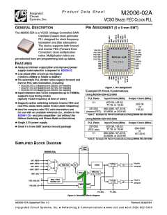
M2006-02A
Integrated
Circuit
Systems, Inc.
VCSO BASED FEC CLOCK PLL
P r o d u c t D a t a S h e e t
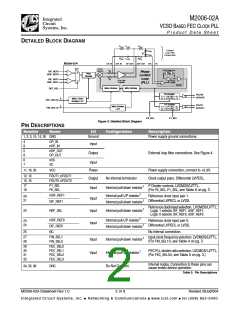
The PLL
Relationship Among Frequencies and Dividers
The PLL uses a phase detector and configurable
dividers to synchronize the output of the VCSO with
selected reference clock.
The VCSO center frequency must be specified at time
of order. The relationship between the VCSO (Fvcso)
frequency, the Mfin divider, the Mfec divider, the Rfec
divider, and the input reference frequency (Fin) is:
The “Mfin Divider” and “Mfec Divider” divide the VCSO
frequency, feeding the result into the phase detector.
Mfec
Rfec
-------------
Fvcso = Fin × Mfin ×
The selected input reference clock is divided by the
“Rfec Divider”. The result is fed into the other input of
the phase detector.
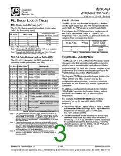
As an example, for the M2006-02A-622.0800, the non-FEC
and inverse-FEC PLL ratios in Table 5 enable use with
these corresponding input reference frequencies:
The phase detector compares its two inputs. It then
outputs pulses to the loop filter as needed to increase or
decrease the VCSO frequency and thereby match and
lock the divider output’s frequency and phase to those
of the input reference clock.
M2006-02A-622.0800
M2006-02A-622.0800
VCSO Clock
Base Input Ref. 1
=
Frequency (MHz)
FEC Ratio
Frequency (MHz)
622.0800
÷
1
/
/
/
/
1
Due to the narrow tuning range of the VCSO
238
237
236
255
255
255
666.5143
669.3266
672.1627
622.08
(+200ppm), appropriate selection of all of the following
are required for the PLL be able to lock: VCSO center
frequency, input frequency, and divider selections.
Table 7: Example FEC PLL Rations and Input Reference Frequencies
Note 1: Input reference clock (“Fin”) can be the base frequency
shown divided by “Mfin” (as shown in Table 4 on pg. 3).
Maintaining PLL Lock:
The narrow tuning range of the VCSO requires that the
input reference frequency must remain suitable for the
current look-up table selection. For example, when
switching between “Inverse FEC ratio” and “Non-FEC
ratio” look-up table selections (see Table 5 on pg. 3), the
input reference frequency must change accordingly in
order for the PLL to lock.
Outputs
The M2006-02A provides a total of two differential
LVPECL output pairs: FOUT1 and FOUT0. Because each
output pair has its own P divider, the FOUT1 pair and the
FOUT0 can output the two different frequencies at the
same time. For example, FOUT1 can output 155.52MHz
while FOUT0 outputs 622.08MHz.
An out-of-lock condition due to an inappropriate
configuration will typically result in the VCSO
operating at its lower or upper frequency rail,
which is approximately 200ppm above or below
the nominal VCSO center frequency.
Any unused output should be left unconnected
(floating) in the system application. This will
minimize output switching current and therefore
minimize noise modulation of the VCSO.
M2006-02A Datasheet Rev 1.0
4 of 8
Revised 28Jul2004
Integrated Circuit Systems, Inc. ● Networking & Communications ● www.icst.com ● tel (508) 852-5400

 ICSI [ INTEGRATED CIRCUIT SOLUTION INC ]