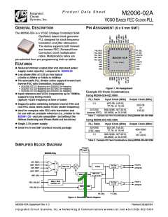
M2006-02A
Integrated
Circuit
Systems, Inc.
VCSO BASED FEC CLOCK PLL
P r o d u c t D a t a S h e e t
Post-PLL Dividers
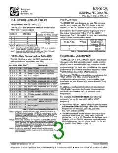
PLL DIVIDER LOOK-UP TABLES
The M2006-02A also features two post-PLL dividers,
one for each output pair. The “P1” divider is for FOUT1
and nFOUT1; the “P0” divider is for FOUT0 and nFOUT0.
Mfin Divider Look-Up Table (LUT)
The FIN_SEL1:0 pins select the feedback divider value
“Mfin” (for Frequency Input).
Each divides the VCSO frequency to produce one of
two output frequencies (1/4 or 1/1 of the VCSO
frequency). The P1_SEL and P0_SEL pins each select the
value for their corresponding divider.
M2006-02A-622.0800
FIN_SEL1:0
Mfin Value
Sample Ref. Freq. (MHz) †
1
1
0
0
1
0
1
0
1 *
4
8
622.08
155.52
77.76
M2006-02A-622.0800
P1_SEL, P0_SEL
P Value
Sample Output
Frequency (MHz)
155.52
32
19.44
Table 4: Mfin Divider Look-Up Table (LUT)
1
0
4
1
Note *: Do not use with FEC_SEL3:0=1100 or 1101 or an excessive
622.08
phase detector frequency will result.
Note †: Example with M2006-02A-622.0800 and “Non-FEC ratio”
Table 6: P Divider Selector, Values, and Frequencies
selection made from Table 5 (FEC_SEL2=1).
FEC PLL Ratio Dividers Look-up Table (LUT)
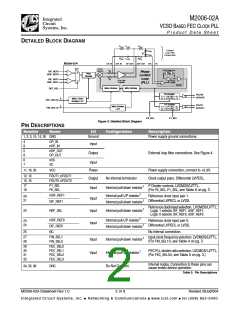
FUNCTIONAL DESCRIPTION
The M2006-02A is a PLL (Phase Locked Loop) based
clock generator that generates output clocks synchro-
nized to one of two selectable input reference clocks.
The FEC_SEL3:0 pins select the FEC feedback and
reference divider values Mfec and Rfec.
Mfec Rfec1
Description
FEC_SEL3:0
An internal high "Q" SAW filter provides low jitter signal
performance and controls the output frequency of the
VCSO (Voltage Controlled SAW Oscillator).
0 0 0 0 236 255 Inverse FEC ratio
0 0 0 1 79
0 0 1 0 14
85 Inverse FEC ratio, equivalent to 237/255
15
Inverse FEC ratio, equivalent to 238/255
Configurable FEC feedback and reference dividers (the
“Mfec Divider” and “Rfec Divider”) provide the
multiplication ratios necessary to accomodate clock
translation for both forward and inverse Forward Error
Correction.
0 0 1 1 239 255 Inverse FEC ratio
Non-FEC ratio, complements 0000 or 1000
2
2
2
2
0 1 0 0 236 236
Non-FEC ratio, complements 0001 or 1001
Non-FEC ratio, complements 0010 or 1010
Non-FEC ratio, complements 0011 or 1011
0 1 0 1 79
0 1 1 0 14
79
14
0 1 1 1 239 239
In addition, a configurable feedback divider (labeled
“Mfin Divider”) provides the broader division options
needed to accomodate various reference clock
frequencies.
1 0 0 0 255 236 FEC ratio (OTU3)
1 0 0 1 85
1 0 1 0 15
79 FEC ratio, equivalent to 255/237 (OTU2)
14 FEC ratio, equivalent to 255/238 (OTU1)
1 0 1 1 255 239 FEC ratio
For example, the M2006-02A-622.0800 (see “Ordering
Information” on pg. 8) has a 622.08MHz VCSO
frequency:
3
1 1 0 0
1 1 0 1
1 1 1 0
1 1 1 1
1
2
4
8
1
2
4
8
Non-FEC ratio Do not use these two settings
with FIN_SEL1:0=11
• The inverse FEC PLL ratios (at top of Table 5) enable
the M2006-02A-622.0800 to accept “base” input reference
frequencies of: 663.7255, 666.5143, 669.3266,
672.1627, and 622.08MHz.
Non-FEC ratio 3
Table 5: FEC PLL Ratio Dividers Look-up Table (LUT)
Note 1: The phase detector frequency (Fpd, which is calculated as
Fref/Rfec) should be above 1.5 MHz to prevent spurs on the
output clock. To ensure the PLL remains locked when using a
recovered clock (such as in loop timing mode), the phase
detector frequency should ideally be about 20MHz, or at least
less than 50 MHz.
Note 2: These table selections use the same or similar Mfec divider
values as the complementary selections noted. This allows the
use of the same loop filter component values and yields the
same PLL loop bandwidth and damping factor values for
complementary selections. Complementary selections can be
actively switched in a given application.
• The Mfin feedback divider enables the actual input
reference clock to be the “base” input frequency
divided by 1, 4, 8, or 32. Therefore, for the base input
frequency of 622.08MHz, the actual input reference
clock frequencies can be: 622.08, 155.52, 77.76, and
19.44MHz. (See Table 4 on pg. 3.)
Note 3: In non-FEC applications, these settings can be used to
optimize phase detector frequency or to actively change PLL
loop bandwidth.
M2006-02A Datasheet Rev 1.0
3 of 8
Revised 28Jul2004
Integrated Circuit Systems, Inc. ● Networking & Communications ● www.icst.com ● tel (508) 852-5400

 ICSI [ INTEGRATED CIRCUIT SOLUTION INC ]