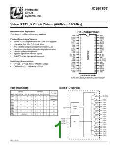
ICS91857
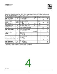
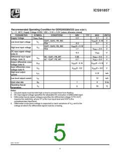
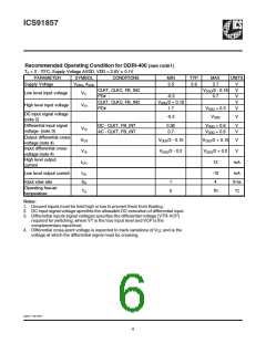
Recommended Operating Condition for DDR200/266/333
(see note1)
TA = 0 - 85°C; Supply Voltage AVDD, VDD = 2.5V 0.2V (unless otherwise stated)
PARAMETER
Supply Voltage
SYMBOL
DDQ, AVDD
CONDITIONS
MIN
2.3
TYP
MAX
2.7
UNITS
V
V
V
V
V
V
CLKT, CLKC, FB_INC
VDDQ/2 - 0.18
0.7
Low level input voltage
High level input voltage
VIL
PD#
-0.3
DDQ/2 + 0.18
1.7
CLKT, CLKC, FB_INC
PD#
V
VIH
V
DDQ + 0.6
VDDQ
DC input signal voltage
(note 2)
-0.3
V
Differential input signal
voltage (note 3)
DC - CLKT, FB_INT
AC - CLKT, FB_INT
0.36
0.7
V
V
DDQ + 0.6
DDQ + 0.6
V
V
VID
VOX
VIX
IOH
Output differential cross-
voltage (note 4)
Input differential cross-
voltage (note 4)
High level output
current
VDDQ/2 - 0.15
VDDQ/2 - 0.2
VDDQ/2 + 0.15
VDDQ/2 + 0.2
0.12
V
V
mA
Low level output current
IOL
SR
TA
12
4
mA
V/ns
°C
Input slew rate
Operating free-air
temperature
1
0
70
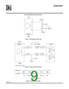
Notes:
1. Unused inputs must be held high or low to prevent them from floating.
2. DC input signal voltage specifies the allowable DC execution of differential input.
3. Differential inputs signal voltages specifies the differential voltage [VTR-VCP]
required for switching, where VT is the true input level and VCP is the
complementary input level.
4. Differential cross-point voltage is expected to track variations of VCC and is the
voltage at which the differential signal must be crossing.
0494C—08/15/05
5

 ICSI [ INTEGRATED CIRCUIT SOLUTION INC ]