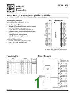
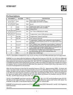
ICS91857
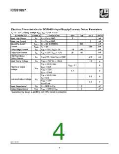
Absolute Maximum Ratings
Supply Voltage (VDD & AVDD) . . . . . . . . . . -0.5V to 4.6V
Logic Inputs . . . . . . . . . . . . . . . . . . . . . . . . . GND –0.5 V to VDD + 0.5 V
Ambient Operating Temperature . . . . . . . . . 0°C to +70°C
Storage Temperature . . . . . . . . . . . . . . . . . . –65°C to +150°C
Stresses above those listed under Absolute Maximum Ratings may cause permanent damage to the device.These
ratings are stress specifications only and functional operation of the device at these or any other conditions above
those listed in the operational sections of the specifications is not implied. Exposure to absolute maximum rating
conditions for extended periods may affect product reliability.
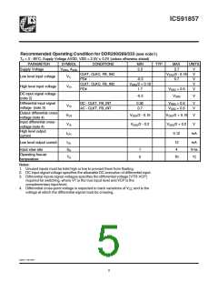
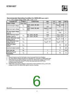
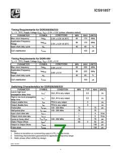
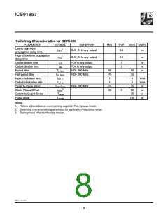
Electrical Characteristics for DDR200/266/333 - Input/Supply/Common Output Parameters
TA = 0 - 70°C; Supply Voltage AVDD, VDD = 2.5V 0.2V (unless otherwise stated)
PARAMETER
SYMBOL
CONDITIONS
VI = VDD or GND
VI = VDD or GND
MIN
5
TYP
MAX
5
UNITS
µA
Input High Current
IIH
IIL
Input Low Current
Operating Supply
Current
µA
IDD2.5 CL = 0pf @ 200MHz
IDDPD CL = 0pf
260
mA
mA
mA
100
Output High Current
Output Low Current
IOH
IOL
VDD = 2.3V, VOUT = 1V
VDD = 2.3V, VOUT = 1.2V
-18
26
-32
35
mA
High Impedance
Output Current
Input Clamp Voltage
IOZ
VIK
VDD=2.7V, Vout=VDD or GND
VDDQ = 2.3V Iin = -18mA
10
mA
-1.2
V
V
V
DD = min to max,
VDDQ - 0.1
1.7
High-level output
voltage
IOH = -1 mA
VOH
VDDQ = 2.3V,
IOH = -12 mA
VDD = min to max
IOL=1 mA
V
V
V
0.1
0.6
Low-level output voltage
VOL
VDDQ = 2.3V
IOH=12 mA
Input Capacitance1
Output Capacitance1
CIN
COUT
VI = GND or VDD
3
3
pF
pF
VOUT = GND or VDD
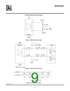
1Guaranteed by design at 170MHz, not 100% tested in production.
0494C—08/15/05
3

 ICSI [ INTEGRATED CIRCUIT SOLUTION INC ]