ICS91857
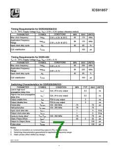
Timing Requirements for DDR200/266/333
TA = 0 - 70°C; Supply Voltage AVDD, VDD = 2.5V 0.2V (unless otherwise stated)
CONDITIONS
PARAMETER
SYMBOL
freqop
MIN
60
MAX UNITS
Max clock frequency
170
170
60
MHz
2.5V 0.2V @ 25°C
Application Frequency
Range
Input clock duty cycle
freqApp
dtin
95
40
MHz
%
2.5V 0.2V @ 25°C
CLK stabilization
TSTAB
100
µs
Timing Requirements for DDRI-400
TA = 0 - 70°C; Supply Voltage AVDD, VDD = 2.6V 0.1V
CONDITIONS
PARAMETER
SYMBOL
freqop
MIN
60
MAX UNITS
Max clock frequency
230
220
60
MHz
MHz
%
2.6V 0.1V
Application Frequency
Range
Input clock duty cycle
freqApp
dtin
95
40
2.6V 0.1V
CLK stabilization
TSTAB
100
µs
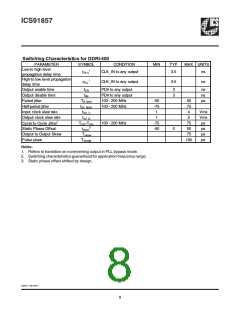
Switching Characteristics for DDR200/266/333
PARAMETER
SYMBOL
CONDITION
MIN
TYP
MAX UNITS
Low-to high level
1
CLK_IN to any output
3.5
3.5
ns
ns
tPLH
propagation delay time
High-to low level propagation
delay time
1
CLK_IN to any output
tPLL
Output enable time
Output disable time
tEN
tdis
PD# to any output
PD# to any output
100 - 200 MHz
3
3
ns
ns
ps
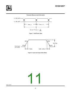
Period jitter
Tjit (per)
t(jit_hper)
t(sir_I)
-75
-75
1
75
75
4
Half-period jitter
100 - 200 MHz
Input clock slew rate
Output clock slew rate
Cycle to Cycle Jitter1
Static Phase Offset
Output to Output Skew
Pulse skew
V/ns
V/ns
ps
t(sl_o)
1
2
Tcyc-Tcyc
100 - 200 MHz
-75
-50
75
50
100
100
3
0
ps
t(spo)
Tskew
ps
Tskewp
ps
Notes:
1. Refers to transition on noninverting output in PLL bypass mode.
2. Switching characteristics guaranteed for application frequency range.
3. Static phase offset shifted by design.
0494C—08/15/05
7

 ICSI [ INTEGRATED CIRCUIT SOLUTION INC ]