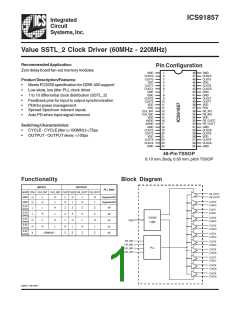
ICS91857
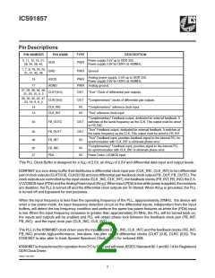
Pin Descriptions
PIN NUMBER
PIN NAME
TYPE
DESCRIPTION
Power supply 2.5V up to DDR 333.
4, 11, 12, 15, 21,
28, 34, 38, 45,
VDD
GND
PWR
Power supply 2.6V for DDR-I at 400MHz.
1, 7, 8, 18, 24, 25,
31, 41, 42, 48
PWR Ground
Analog power supply, 2.5V up to DDR 333.
Power supply 2.6V for DDR-I at 400MHz.
PWR Analog ground.
16
AVDD
PWR
17
AGND
27, 29, 39, 44, 46,
22, 20, 10, 5, 3
CLKT(9:0)
OUT
OUT
"True" Clock of differential pair outputs.
26, 30, 40, 43, 47,
23, 19, 9, 6, 2
CLKC(9:0)
"Complementary" clocks of differential pair outputs.
14
13
CLK_INC
CLK_INT
IN
IN
"Complementary" reference clock input
"True" reference clock input
"Complementary" Feedback output, dedicated for external feedback. It
switches at the same frequency as the CLK. This output must be wired
to FB_INC.
33
FB_OUTC
OUT
"True" Feedback output, dedicated for external feedback. It switches at
the same frequency as the CLK. This output must be wired to FB_INT.
32
36
FB_OUTT
FB_INT
OUT
IN
"True" Feedback input, provides feedback signal to the internal PLL for
synchronization with CLK_INT to eliminate phase error.
"Complementary" Feedback input, provides signal to the internal PLL
for synchronization with CLK_INC to eliminate phase error.
35
37
FB_INC
PD#
IN
IN
Power Down. LVCMOS input
This PLL Clock Buffer is designed for a VDD of 2.5V, an AVDD of 2.5V and differential data input and output levels.
ICS91857 is a zero delay buffer that distributes a differential clock input pair (CLK_INC, CLK_INT) to ten differential
pairofclockoutputs(CLKT[0:9], CLKC[0:9])andonedifferentialpairfeedbackclockoutput(FB_OUT, FB_OUTC).The
clock outputs are controlled by the input clocks (CLK_INC, CLK_INT), the feedback clocks (FB_INT, FB_INC) the 2.5-
VLVCMOSinput(PD#)andtheAnalogPowerinput(AVDD).Wheninput(PD#)islowwhilepowerisapplied, thereceivers
are disabled, the PLL is turned off and the differential clock outputs areTri-Stated.When AVDD is grounded, the PLL
is turned off and bypassed for test purposes.
When the input frequency is less than the operating frequency of the PLL, appproximately 20MHz, the device will
enter a low power mode. An input frequency detection circuit on the differential inputs, independent from the input
buffers, will detect the low frequency condition and perform the same low power features as when the (PD#) input
is low. When the input frequency increases to greater than approximately 20 MHz, the PLL will be turned back on,
the inputs and outputs will be enabled and PLL will obtain phase lock between the feedback clock pair (FB_INT,
FB_INC) and the input clock pair (CLK_INC, CLK_INT).
The PLL in the ICS91857 clock driver uses the input clocks (CLK_INC, CLK_INT) and the feedback clocks (FB_INT,
FB_INC) provide high-performance, low-skew, low-jitter output differential clocks (CLKT [0:9], CLKC [0:9]). The
ICS91857 is also able to track Spread Spectrum Clock (SSC) for reduced EMI.
ICS91857 ischaracterizedforoperationfrom0°Cto70°CandwillmeetJEDECStandard82-1and82-1AforRegistered
DDRClockDriver.
0494C—08/15/05
2

 ICSI [ INTEGRATED CIRCUIT SOLUTION INC ]