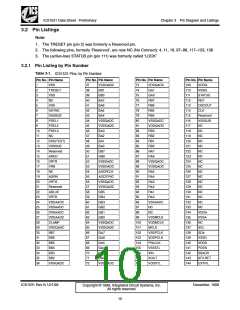
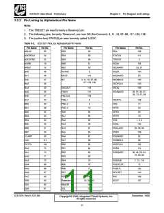
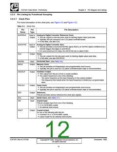
ICS1531 Data Sheet - Preliminary
Chapter 3 Pin Diagram and Listings
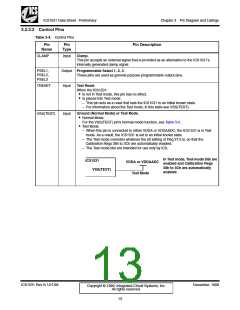
3.2.3.2 Control Pins
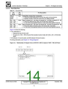
Table 3-4. Control Pins
Pin
Pin
Pin Description
Name
Type
CLAMP
Input
Clamp.
This pin accepts an external signal that is provided as an alternative to the ICS1531’s
internally generated clamp signal.
PSEL1,
PSEL2,
PSEL3
Output Programmable Select 1, 2, 3.
These pins are used as general-purpose programmable output pins.
TRESET
Input
Test Reset.
When the ICS1531:
• Is not in Test mode, this pin has no effect.
• Is placed into Test mode:
– This pin acts as a reset that sets the ICS1531 to an initial known state.
– For information about the Test mode, in this table see VSS(TEST).
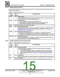
G•roNuonrdm(aNloMromdael.Mode) or Test Mode.
VSS(TEST)
Input
For the VSS(TEST) pin’s Normal-mode function, see Table 3-4.
• Test Mode.
– When this pin is connected to either VDDA or VDDAADC, the ICS1531 is in Test
mode. As a result, the ICS1531 is set to an initial known state.
– The Test mode overrides whatever the bit setting of Reg 37:3 is, so that the
Calibration Regs 38h to 3Ch are automatically enabled.
– The Test mode bits are intended for use only by ICS.
In Test mode, Test-mode bits are
enabled and Calibration Regs
ICS1531
VDDA or VDDAADC
38h to 3Ch are automatically
enabled.
VSS(TEST)
Test Mode
ICS1531 Rev N 12/1/99
December, 1999
Copyright © 1999, Integrated Circuit Systems, Inc.
All rights reserved.
13

 ICSI [ INTEGRATED CIRCUIT SOLUTION INC ]