ICS1531 Data Sheet - Preliminary
Chapter 3 Pin Diagram and Listings
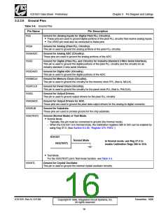
3.2.3.7 Power Pins
Table 3-9. Power Pins
Pin Name
Pin Description
(3.3 V) Supply for Analog (Pixel PLL Circuitry).
VDDA
This pin supplies 3.3 V to the analog portions of the pixel PLL circuitry.
VDDAADC
VDDD
(3.3 V) Supply for Analog ADC (Circuitry).
These pins supply 3.3 V to the analog portions of the ADC.
(3.3 V) Supply for Digital (Pixel PLL and Industry-Standard 2-Wire Serial Bus) Circuitry.
This pin supplies 3.3 V to the digital pixel PLL and circuitry for an industry-standard 2-wire serial bus
interface.
VDDDADC
VDDMCLK
VDDPCLK
VDDQ
(3.3 V) Supply for Digital ADC (Circuitry).
This pin supplies 3.3 V to digital portions of the ADC.
(3.3 V) Supply for Memory Clock.
This pin supplies 3.3 V to the memory clock PLL circuitry.
(3.3 V) Supply for Panel Clock.
This pin supplies 3.3 V to the panel clock PLL circuitry.
(3.3 V) Supply for Output Drivers.
This pin supplies 3.3 V to the output driver circuitry for the pixel PLL.
VDDQADC
VDDXTL
VRB
(3.3 V) Supply for Output Drivers for Analog-to-Digital Converter.
These pins supply 3.3 V to the pixel data output drivers of the ADC.
(3.3V) Supply for Crystal Oscillator.
This pin supplies 3.3 V to the internal crystal oscillator circuitry.
Voltage Reference Bottom.
The ADC uses this pin as a bottom reference voltage. Typically, this pin is grounded.
V•oltTahgeeARDeCfeuresnecsethTeospe Bpilnuse,aGs raeneanl,teRrneadtive to the blue, green, and red top reference voltages
VRTB,
VRTG,
VRTR
from the internal DACs.
• Each of these pins must connect to its own separate bypass capacitor.
ICS1531 Rev N 12/1/99
December, 1999
Copyright © 1999, Integrated Circuit Systems, Inc.
All rights reserved.
17

 ICSI [ INTEGRATED CIRCUIT SOLUTION INC ]