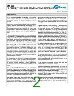
iC-JX
16-FOLD 24 V HIGH-SIDE DRIVER WITH µC INTERFACE
Rev C1, Page 4/36
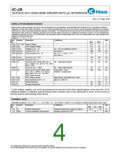
ABSOLUTE MAXIMUM RATINGS
Beyond these values damage may occur; device operation is not guaranteed. Absolute Maximum Ratings are no Operating Conditions.
Integrated circuits with system interfaces, e.g. via cable accessible pins (I/O pins, line drivers) are per principle endangered by injected
interferences, which may compromise the function or durability. The robustness of the devices has to be verified by the user during system
development with regards to applying standards and ensured where necessary by additional protective circuitry. By the manufacturer
suggested protective circuitry is for information only and given without responsibility and has to be verified within the actual system with
respect to actual interferences.
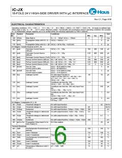
(Legend: x = 1..16, y = 1..4)
Item Symbol
No.
Parameter
Conditions
Unit
Min.
-0.3
-0.3
-10
Max.
6
G001 VCC, VDD Supply Voltage
V
V
G002 VBy
Driver Supply Voltage
40
G003 V(IOx)
G004 Idc(IOx)
G005 Ipk(IOx)
Voltages at IO1...16
Current in IO1...16
IOx = off; see additional remark 1
see Figure 1
40
V
-500
-1.0
150
mA
A
Pulse current in IO1...16
IOx = hi, τ = 2 ms, T ≤ 2 s
see Figure 2
G006 Imax()
Current in VCC, VDD
-100
-8
100
8
mA
A
G007 Imax(VBy) Current in VB1...4
G008 Ic()
Current in NCS, NWR, NRD, A0...4,
D0...7, NRES, CLK, BLFQ, POE, NSP,
RSET, VREF
D0...7 with input function
D0...7 with output function
-20
20
mA
G009 I()
Current in D0...7, NINT,
-25
25
mA
mA
G010 Ilu()
Pulse current in NCS, NWR, NRD,
A0...4, D0...7, NRES, CLK, BLFQ,
NINT, NSP, POE, IO1...16, RSET,
VREF (latch up test)
Pulse width < 10 µs,
all inputs / outputs open
-100
100
G011 Vd()
G012 Vb()
G013 Tj
ESD-voltage, all pins
Burst transients at IO1...16
Chip temperature
HBM 100 pF discharged over 1.5 kΩ
2
kV
kV
°C
°C
after IEC 1000-4-4
4
-40
-40
150
150
G014 Ts
Storage temperature
1)
If the voltage supplies can not be guaranteed to be present at the time signals appear at the pins IO1..IO16,
additional diodes or sufficient current limiting ohmic resistors have to be connected in series to the IO-pins to
prevent reverse back biasing of the device.
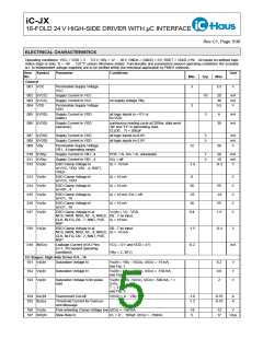
THERMAL DATA
Operating conditions: VCC = VDD = 3 ... 5.5 V, VBy = 12 ... 36 V, GNDA = GNDD = 0 V, all inputs on defined logic states (high or low)
Item Symbol
No.
Parameter
Conditions
Unit
Min. Typ. Max.
-40 85
T01 Ta
Ambient temperature
extended temperature range on request
package mounted on PCB
°C
T02 Rthja
Thermal resistance chip/ambient
55
K/W
All voltages are referenced to ground unless otherwise stated.
All currents flowing into the device pins are positive; all currents flowing out of the device pins are negative.

 ICHAUS [ IC-HAUS GMBH ]