iC-JX
16-FOLD 24 V HIGH-SIDE DRIVER WITH µC INTERFACE
Rev C1, Page 3/36
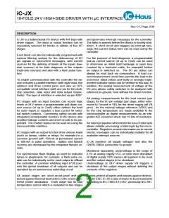
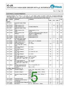
PACKAGES MQFP52 to JEDEC Standard
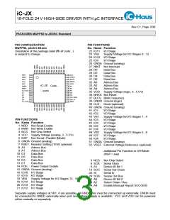
PIN CONFIGURATION
PIN FUNCTIONS
MQFP52, pitch 0.65 mm
Orientation of the package label ( JX code...)
is subject to change.
No. Name Function
22 IO11 I/O Stage
23 VB3
Supply Voltage for I/O Stages 9...12
24 IO10 I/O Stage
25 IO9
I/O Stage
26 GNDA Ground (analog)
27 NINT Not Interrupt
28 D0
29 D2
30 D4
31 D6
32 A0
33 A2
34 A4
Data Bus
Data Bus
Data Bus
Data Bus
Adress Bus
Adress Bus
Adress Bus
1
2
39
38
37
36
35
34
33
32
31
30
29
28
27
CLK
NRD
NWR
NCS
VCC
NSP
GNDD
BLFQ
NRES
VDD
A4
3
4
5
iC-JX
...
...yyww
6
Code...
GNDA
RSET
A3 / SCK
A1
7
A2
8
A0
35 VDD Supply Voltage (logic, 3...5.5 V)
36 NRES Not Reset
37 BLFQ Blink Frequency
38 GNDD Ground (logic)
9
D6
10
11
D4
D7
D5
D2 / SOB
D0 / SI
NINT
12
13
D3
D1 / SOC
39 CLK
Clock (optional)
40 GNDA Ground (analog)
41 IO1
42 IO2
43 VB1
44 IO3
45 IO4
46 IO5
47 IO6
48 VB2
49 IO7
50 IO8
I/O Stage
I/O Stage
Supply Voltage for I/O Stages 1...4
I/O Stage
I/O Stage
I/O Stage
I/O Stage
Supply Voltage for I/O Stages 5...8
PIN FUNCTIONS
No. Name Function
1 NRD Not Read Enable
2 NWR Not Write Enable
3 NCS Not Chip Select
4 VCC Supply Voltage (analog, 3...5.5 V)
5 NSP Not Serial / Parallel (Mode)
6 GNDA Ground (analog)
I/O Stage
I/O Stage
51 GNDA Ground (analog)
52 VREF External Voltage Reference (optional)
7 RSET Resistor Setting (10 kΩ optional)
8 A3
9 A1
10 D7
11 D5
12 D3
13 D1
Adress Bus
Adress Bus
Data Bus
Data Bus
Data Bus
Data Bus
Additional Pin Function in SPI Mode
(NSP = low)
3 NCS Not Chip Select
8 SCK Serial Clock
14 POE Power Output Enable
15 GNDA Ground (analog)
16 IO16 I/O Stage
9 A1
13 SOC Serial Out Chain
28 SI Serial In
29 SOB Serias Out Bus
Device ID Bit 1
17 IO15 I/O Stage
18 VB4
Supply Voltage for I/O Stages 13...16
32 A0
33 A2
34 A4
Device ID Bit 0
Select Chain / Bus
Enable Interrupt Report SOC/SOB
19 IO14 I/O Stage
20 IO13 I/O Stage
21 IO12 I/O Stage
Separate supply voltages at VB1..4 are possible. All GNDA pins must be connected up externally. GNDA must
be connected to GNDD externally when just one voltage supply is available. VCC and VDD can be powered
either mutually or separately.

 ICHAUS [ IC-HAUS GMBH ]