iC-JX
16-FOLD 24 V HIGH-SIDE DRIVER WITH µC INTERFACE
Rev C1, Page 9/36
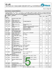
ELECTRICAL CHARACTERISTICS
Operating conditions: VCC = VDD = 3 ... 5.5 V, VBy = 12 ... 36 V, GNDA = GNDD = 0 V, RSET = 10 kΩ ±1% . All inputs on defined logic
states (high or low), Tj = -40 ... 125 °C unless otherwise stated. Functionality and parameters beyond operating conditions (for example
w.r. to independent voltage supplies) are to be verified within the individual application by FMEA methods.
Item Symbol
No.
Parameter
Conditions
Unit
Min.
Typ.
Max.
740
DR3IO,0
Relative value using VR3 range
(internal reference)
SELAD = ’0b100’, EME = ’0b0’, SVREF = 0;
DR3IO,0 = D3IO,0(V) / D3IO,0
V(IOx) = 0.3V
48
14.5
50
16
52
18.5
%
%
V(IOx) = 0.1V
741
742
D4IO,0
Digital value using VR4 range
(internal reference)
SELAD = ’0b100’, EME = ’0b1’, SVREF = 0,
V(IOx) = 5.0V
790
840
1022
DR4IO,0
Relative value using VR4 range
(internal reference)
SELAD = ’0b100’, EME = ’0b1’, SVREF = 0;
DR4IO,0 = D4IO,0(V) / D4IO,0
V(IOx) = 2.5V
48
9.5
50
11.5
52
14
%
%
V(IOx) = 0.6V
743
744
D5IO,0
Digital value using VR5 range
(internal reference)
SELAD = ’0b011’, SVREF = 0
V(IOx) = 36.0V
810
870
1022
DR5IO,0
Relative value using VR5 range
(internal reference)
SELAD = ’0b011’, SVREF = 0;
DR5IO,0 = D5IO,0(V) / D5IO,0
V(IOx) = 24.0V
64.6
11.8
66.6
13.8
68.6
15.8
%
%
V(IOx) = 5.0V
745 DCIO,0
746
Digital value of current measure- SELAD = ’0b001’, SVREF = 0, I(IOx) = 150mA
ment (internal reference)
720
820
1022
DRCIO,0
Digital value of current
SELAD = ’0b001’, SVREF = 0;
DRCIO,0 = DCIO,0(I) / DCIO,0
I(IOx) = 75mA
measurement (internal reference)
48
51
54
%
%
I(IOx) = 15mA
6.2
9.2
12.2
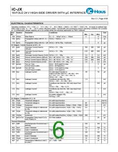
Input RSET
B01 V(RSET) Voltage at RSET
B02 R(RSET) Range value for RSET
Burst-Indication
1.15
9
1.22
10
1.30
14
V
kΩ
C01 VSPon
C02 VSPoff
C03 tpoff
Input On-Threshold for burst
recognition
1.3
1.4
2
2.9
3
V
V
Input Off-Threshold for Burst-
recognition
Delay time to Reset after spike at Spike duration: 10 ns
VCC, VDD
110
µs
Pin monitoring GNDA, GNDD
H01 Vt()gnd Threshold voltage for open ciruit
detection on pins GNDA, GNDD
35
1
65
15
mV
µs
H02 tmin()gnd Minimum duration for open circuit V(GNDA,GNDD) = 0 V ... Vt()gnd
detection
H03 tpoff
Delay time to reset after open
µs
circuit detection at GNDA, GNDD
Undervoltage detection VB
I01 VByon
Undervoltage message VB1...4
on
10.6
10.0
11.2
10.6
11.8
11.2
V
V
I02 VByoff
Undervoltage message VB1...4
off
I03 VByhys
I04 tmin()lv
Hysteresis
VByhys = VByon - VByoff
VBy = 0.8 V ... VByoff
400
1
mV
µs
Minimum duration for Power-
Down detection
I05 tpoff
Delay time for undervoltage mes-
sage VB1...4
6
2
µs
V
µC-Intrface, I/O-Logic, Frequency divider, Interrupt
K01 Vt()hi
Threshold voltage High at
Schmitt-Trigger-Inputs
D0...7 with input function
NCS, NWR, NRD, A0...4, NRES,
CLK, BLFQ, D0...7, NSP, POE

 ICHAUS [ IC-HAUS GMBH ]