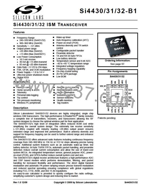
Si4430/31/32-B1
the output from the - modulator. The tuning resolution is sufficient to tune to the commanded frequency with a
maximum accuracy of 312.5 Hz anywhere in the range between 240–960 MHz.
5.6.1. VCO
The output of the VCO is automatically divided down to the correct output frequency depending on the hbsel and
fb[4:0] fields in "Register 75h. Frequency Band Select." In receive mode, the LO frequency is automatically shifted
downwards by the IF frequency of 937.5 kHz, allowing transmit and receive operation on the same frequency. The
VCO integrates the resonator inductor and tuning varactor, so no external VCO components are required.
The VCO uses a capacitance bank to cover the wide frequency range specified. The capacitance bank will
automatically be calibrated every time the synthesizer is enabled. In certain fast hopping applications this might not
be desirable so the VCO calibration may be skipped by setting the appropriate register.
5.7. Power Amplifier
The Si4432 contains an internal integrated power amplifier (PA) capable of transmitting at output levels between –1
and +20 dBm. The Si4431/4430 contains a PA which is capable of transmitting output levels between –8 to
+13 dBm. The PA design is single-ended and is implemented as a two stage class CE amplifier with a high
efficiency when transmitting at maximum power. The PA efficiency can only be optimized at one power level.
Changing the output power by adjusting txpow[2:0] will scale both the output power and current but the efficiency
will not remain constant. The PA output is ramped up and down to prevent unwanted spectral splatter.
In the Si4431, the TX and RX may be tied directly. See the TX/RX direct-tie reference design available on the
Silicon Labs website. for more details. When the direct tie is used, the lna_sw bit in “Register 6Dh. TX Power” must
be set.
5.7.1. Output Power Selection
The output power is configurable in 3 dB steps with the txpow[2:0] field in "Register 6Dh. TX Power." Extra output
power can allow the use of a cheaper smaller antenna, greatly reducing the overall BOM cost. The higher power
setting of the chip achieves maximum possible range, but of course comes at the cost of higher TX current
consumption. However, depending on the duty cycle of the system, the effect on battery life may be insignificant.
Contact Silicon Labs Support for help in evaluating this tradeoff.
D7
D6
D5
D4
D3
D2
D1
D0
POR
Def.
Add R/W Function/D
escription
6D R/W
TX Power
papeakval papeaken papeaklv[1] papeaklv[0] lna_sw txpow[2] txpow[1] txpow[0] 18h
txpow[2:0]
000
Si4432 Output Power
+1 dBm
001
+2 dBm
010
+5 dBm
011
+8 dBm
100
+11 dBm
101
+14 dBm
110
+17 dBm
111
+20 dBm
txpow[2:0]
000
Si4431/30 Output Power
–8 dBm
001
–5 dBm
010
–2 dBm
011
+1 dBm
100
+4 dBm
101
+7 dBm
110
+10 dBm
111
+13 dBm
Rev 1.0
39

 IBM [ IBM ]