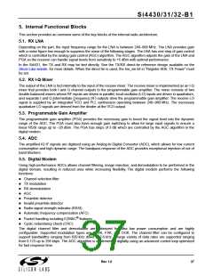
Si4430/31/32-B1
5. Internal Functional Blocks
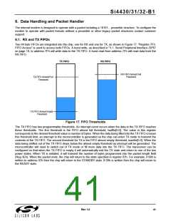
This section provides an overview some of the key blocks of the internal radio architecture.
5.1. RX LNA
Depending on the part, the input frequency range for the LNA is between 240–960 MHz. The LNA provides gain
with a noise figure low enough to suppress the noise of the following stages. The LNA has one step of gain control
which is controlled by the analog gain control (AGC) algorithm. The AGC algorithm adjusts the gain of the LNA and
PGA so the receiver can handle signal levels from sensitivity to +5 dBm with optimal performance.
In the Si4431, the TX and RX may be tied directly. See the TX/RX direct-tie reference design available on the
Silicon Labs website. for more details. When the direct tie is used, the lna_sw bit in “Register 6Dh. TX Power” must
be set.
5.2. RX I-Q Mixer
The output of the LNA is fed internally to the input of the receive mixer. The receive mixer is implemented as an I-Q
mixer that provides both I and Q channel outputs to the programmable gain amplifier. The mixer consists of two
double-balanced mixers whose RF inputs are driven in parallel, local oscillator (LO) inputs are driven in quadrature,
and separate I and Q Intermediate Frequency (IF) outputs drive the programmable gain amplifier. The receive LO
signal is supplied by an integrated VCO and PLL synthesizer operating between 240–960 MHz. The necessary
quadrature LO signals are derived from the divider at the VCO output.
5.3. Programmable Gain Amplifier
The programmable gain amplifier (PGA) provides the necessary gain to boost the signal level into the dynamic
range of the ADC. The PGA must also have enough gain switching to allow for large input signals to ensure a
linear RSSI range up to –20 dBm. The PGA has steps of 3 dB which are controlled by the AGC algorithm in the
digital modem.
5.4. ADC
The amplified IQ IF signals are digitized using an Analog-to-Digital Converter (ADC), which allows for low current
consumption and high dynamic range. The bandpass response of the ADC provides exceptional rejection of out of
band blockers.
5.5. Digital Modem
Using high-performance ADCs allows channel filtering, image rejection, and demodulation to be performed in the
digital domain, resulting in reduced area while increasing flexibility. The digital modem performs the following
functions:
Channel selection filter
TX modulation
RX demodulation
AGC
Preamble detector
Invalid preamble detector
Radio signal strength indicator (RSSI)
Automatic frequency compensation (AFC)
®
Packet handling including EZMAC features
Cyclic redundancy check (CRC)
The digital channel filter and demodulator are optimized for ultra low power consumption and are highly
configurable. Supported modulation types are GFSK, FSK, and OOK. The channel filter can be configured to
support bandwidths ranging from 620 kHz down to 2.6 kHz. A large variety of data rates are supported ranging
from 0.123 up to 256 kbps. The AGC algorithm is implemented digitally using an advanced control loop optimized
for fast response time.
Rev 1.0
37

 IBM [ IBM ]