IBM PowerPC 403GCX
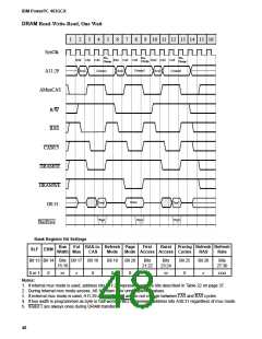
DMA Buffered Single Transfer from Peripheral to 3-Cycle DRAM
1
2
3
4
5
6
7
8
9
10 11 12
SysClk
BIU
Req
DMA
Ack
Pre-
Charge
Sync
Sync
RAS
CAS
CAS
DMAR
DMAA
A11:29
R/W
Row
Column
RAS
CAS0:3
DRAMOE
DRAMWE
D0:31
Data
Data
OE
WBE0:3
Bank Register Bit Settings
Bus Ext RAS-to- Refresh Page
Width Mux
First
Burst
Prechg Refresh Refresh
SLF ERM
CAS
Mode
Mode Access Access Cycles
RAS
Rate
Bit 13 Bit 14 Bits Bit 17 Bit 18
15:16
Bit 19
Bit 20
Bits
21:22
Bits
23:24
Bit 25
Bit 26
Bits
27:30
0 or 1
0
10
0
0
0
0
01
xx
0
x
xxxx
DMA Control Register Bit Settings
Transfer Direction Transfer Width Transfer Mode PeripheralSetup Peripheral Wait Peripheral Hold
Bit 2
1
Bits 4:5
10
Bits 9:10
00
Bits 11:12
00
Bits 13:18
00 0000
Bits 19-21
000
Notes:
1. DMAR must be inactive in cycle 9 to guarantee a single transfer.
2. This waveform assumes that the internal address mux is used.
3. CAS0 is used for byte accesses, CAS0:1 for halfwords, and CAS0:3 for fullwords.
50

 IBM [ IBM ]