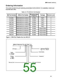
IBM PowerPC 403GCX
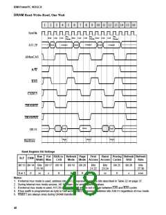
DMA Fly-By Single Transfer, Write to 3-Cycle DRAM
1
2
3
4
5
6
7
8
9
10
11
12
SysClk
DMAR
DMAA
Pre-
BIUReq RAS
S=0
CAS
Sync
Sync
CAS
Charge
(S = peripheral setup time)
S=1
S=2
DMADXFER
A11:29
Row
Column
R/W
RAS
CAS0:3
DRAMOE
DRAMWE
D0:31
Data
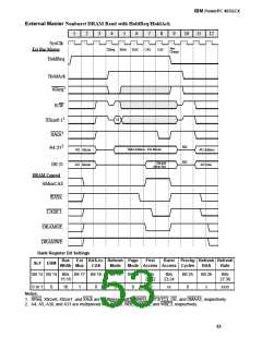
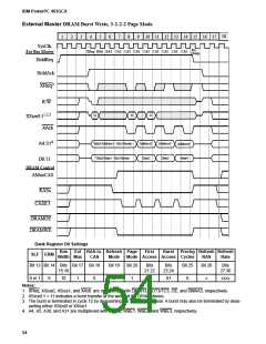
Bank Register Bit Settings
Bus
Width Mux
Ext RAS-to- Refresh Page
First
Burst
Prechg Refresh Refresh
SLF ERM
CAS
Mode Mode Access Access Cycles
RAS
Rate
Bit 13 Bit 14 Bits Bit 17 Bit 18
15:16
Bit 19
Bit 20
Bits
21:22
Bits
23:24
Bit 25
Bit 26
Bits
27:30
0 or 1
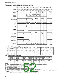
DMA Control Register Bit Settings
Transfer Direction Transfer Width Transfer Mode PeripheralSetup Peripheral Wait Peripheral Hold
0
10
0
0
0
0
01
xx
0
x
xxxx
Bit 2
1
Bits 4:5
10
Bits 9:10
01
Bits 11:12
Note 3
Bits 13:18
xx xxxx
Bits 19-21
xxx
Notes:
1. DMAR must be inactive in cycle 7 (last DMAA cycle) to guarantee a single transfer.
2. Peripheral data bus width must match DRAM bus width.
3. See diagram for settings.
4. This waveform assumes that the internal address mux is used.
5. CAS0 is used for byte accesses, CAS0:1 for halfwords, and CAS0:3 for fullwords.
51

 IBM [ IBM ]