APCPCWM_4828539:WP_0000001WP_0000001
1
H27(U_S)4G8_6F2D
4 Gbit (512M x 8 bit) NAND Flash
1 Summary Description
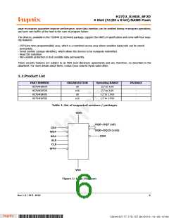
H27(U_S)4G8_6F2D series is a 512Mx8bit with spare 16Mx8 bit capacity.
The device is offered in 3.0/1.8 Vcc Power Supply, and with x8 and x16 I/O interface
Its NAND cell provides the most cost-effective solution for the solid state mass storage market.
The memory is divided into blocks that can be erased independently so it is possible to preserve valid data while old
data is erased.
The device contains 4096 blocks, composed by 64 pages.
Memory array is split into 2 planes, each of them consisting of 2048 blocks.
Like all other 2KB - page NAND Flash devices, a program operation allows to write the 2112-byte page in typical
200us(3.3V) and an erase operation can be performed in typical 3.5ms on a 128K-byte block.
In addition to this, thanks to multi-plane architecture, it is possible to program 2 pages at a time (one per each plane)
or to erase 2 blocks at a time (again, one per each plane). As a consequence, multi-plane architecture allows program
time to be reduced by 40% and erase time to be reduction by 50%. In case of multi-plane operation, there is small deg-
radation at 1.8V application in terms of program/erase time.
The multiplane operations are supported both with traditional and ONFI 1.0 protocols.
Data in the page can be read out at 25ns (3V version) and 45nsec (1.8V version) cycle time per byte. The I/O pins
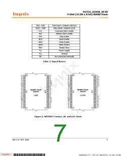
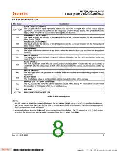
serve as the ports for address and data input/output as well as command input. This interface allows a reduced pin
count and easy migration towards different densities, without any rearrangement of footprint.
Commands, Data and Addresses are synchronously introduced using CE#, WE#, ALE and CLE input pin.
The on-chip Program/Erase Controller automates all read, program and erase functions including pulse repetition,
where required, and internal verification and margining of data.
A WP# pin is available to provide hardware protection against program and erase operations.
The output pin RB# (open drain buffer) signals the status of the device during each operation. In a system with multi-
ple memories the RB# pins can be connected all together to provide a global status signal.
Each block can be programmed and erased up to 100,000 cycles with ECC (error correction code) on. To extend the life-
time of Nand Flash devices, the implementation of an ECC is mandatory.
The chip supports CE# don't care function. This function allows the direct download of the code from the NAND Flash
memory device by a microcontroller, since the CE# transitions do not stop the read operation.
In addition, device supports ONFI 1.0 specification.
The copy back function allows the optimization of defective blocks management: when a page program operation fails
the data can be directly programmed in another page inside the same array section without the time consuming serial
data insertion phase. Copy back operation automatically executes embedded error detection operation: 1 bit error out
of every 528-byte (x8) or 1 bit error out of every 264-word (x16) can be detected. With this feature it is no longer nec-
essary to use an external to detect copy back operation errors.
Multiplane copy back is also supported, both with traditional and ONFI 1.0 protocols. Data read out after copy back read
(both for single and multiplane cases) is allowed.
In addition, Cache program and multi cache program operations improve the programing throughput by programing
data using the cache register.
The devices provide two innovative features: page re-program and multiplane page re-program. The page re-program
allows to re-program one page. Normally, this operation is performed after a previously failed page program operation.
Similarly, the multiplane page re-program allows to re-program two pages in parallel, one per each plane. The first page
must be in the first plane while the second page must be in the second plane; the multiplane page re-program opera-
tion is performed after a previously failed multiplane page program operation. The page re-program and multiplane
Rev 1.4 / OCT. 2010
5
B34416/177.179.157.84/2010-10-08 10:08
*ba53f20d-240c*

 HYNIX [ HYNIX SEMICONDUCTOR ]