APCPCWM_4828539:WP_0000001WP_0000001
1
H27(U_S)4G8_6F2D
4 Gbit (512M x 8 bit) NAND Flash
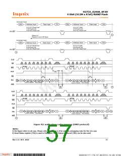
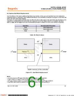
8.3 Bad Block Management
Devices with Bad Blocks have the same quality level and the same AC and DC characteristics as devices where all the
blocks are valid. A Bad Block does not affect the performance of valid blocks because it is isolated from the bit line and
common source line by a select transistor. The devices are supplied with all the locations inside valid blocks
erased(FFh). The Bad Block Information is written prior to shipping. Any block where the 1st Byte in the spare area of
the 1st or 2nd th page (if the 1st page is Bad) does not contain FFh is a Bad Block. The Bad Block Information must be
read before any erase is attempted as the Bad Block Information may be erased. For the system to be able to recog-
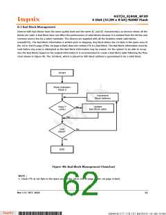
nize the Bad Blocks based on the original information it is recommended to create a Bad Block table following the flow-
chart shown in Figure 48. The 1st block, which is placed on 00h block address is guaranteed to be a valid block.
67$57
%ORFNꢃ$GGUHVV
%ORFNꢃꢉ
,QFUHPHQW
%ORFNꢃ$GGUHVV
'DWD ꢋꢁꢍ
))K"
8SGDWH
%DGꢃ%ORFNꢃWDEOH
1R
1R
<HV
/DVW
EORFN"
<HV
(1'
Figure 48: Bad Block Management Flowchart
NOTE :
1. Check FFh at 1st Byte in the spare area of the 1st or 2nd th page (if the 1st page is Bad).
Rev 1.4 / OCT. 2010
62
B34416/177.179.157.84/2010-10-08 10:09
*ba53f20d-240c*

 HYNIX [ HYNIX SEMICONDUCTOR ]