APCPCWM_4828539:WP_0000001WP_0000001
1
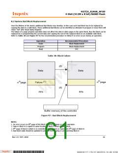
H27(U_S)4G8_6F2D
4 Gbit (512M x 8 bit) NAND Flash
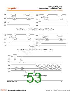
Command Input
82ꢇ
11ꢇ
82ꢇ
Address Input
Data Input
15ꢇ
Address Input
Data Input
A13~A17:Fixed”Loꢆ”
A18:Fixed”Loꢆ”
A19~A31:Fixed”Loꢆ”
A13~A17:ꢀaꢄid
A18:Fixed”Loꢆ”
A19~A31:Fixed”Loꢆ”
t
t
PCBSY
DBSY
RY/BY
1
Return to 1
Repeat a max oꢁ 63 times
Command Input
11ꢇ
82ꢇ
Address Input
Data Input
12ꢇ
Address Input
Data Input
82ꢇ
A13~A17:Fixed”Loꢆ”
A18:Fixed”Loꢆ”
A19~A31:Fixed”Loꢆ”
A13~A17:ꢀaꢄid
A18:Fixed”Loꢆ”
A19~A31:Fixed”Loꢆ”
t
t
PROG
DBSY
RY/BY
1
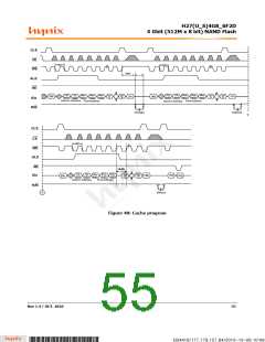
CLE
CE
tWC
tWB
WE
ALE
tWB
RE
tADL
tADL
IOx
Din
N
Din
M
Din
N
Din
M
Col.
Add1
Col.
Add2
Row
Add1
Row
Add2
Row
Add3
Col.
Add1
Col.
Add2
Row
Add1
Row
Add2
Row
Add3
80h
11h
15h
80h
Coꢄumn Address
Roꢆ Address
Roꢆ Address
Coꢄumn Address
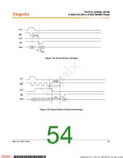
R/B
1
tDBSY
tCBSY
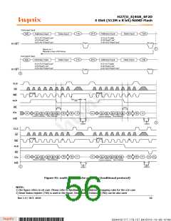
CLE
CE
tWC
tWB
WE
ALE
RE
Din
N
Din
M
Din
N
Din
M
Col.
Add1
Col.
Add2
Row
Add1
Row
Add2
Row
Add3
Col.
Add1
Col.
Add2
Row
Add1
Row
Add2
Row
Add3
80h
80h
11h
10h
I/O
Q
F1h
IOx
Coꢄumn Address
Roꢆ Address
Roꢆ Address
Coꢄumn Address
R/B
1
tPROG
tDBSY
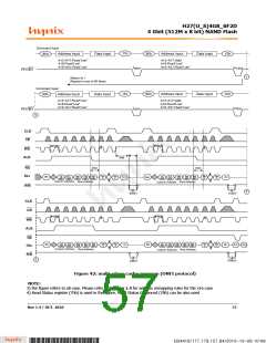
Figure 42: multi-plane cache program (ONFI protocol)
NOTE:
3) the figure refers to x8 case. Please refer to Section 1.4 for address remapping rules for the x16 case
4) Read Status register (70h) is used in the figure. Read Status Enhanced (78h) can be also used
Rev 1.4 / OCT. 2010
57
B34416/177.179.157.84/2010-10-08 10:08
*ba53f20d-240c*

 HYNIX [ HYNIX SEMICONDUCTOR ]