APCPCWM_4828539:WP_0000001WP_0000001
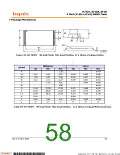
1
H27(U_S)4G8_6F2D
4 Gbit (512M x 8 bit) NAND Flash
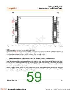
x8
x8
R/Vss
R
R
R
1
2
3
4
5
6
7
8
48
47
46
45
44
R
R
R
R/B4#
R/B3#
R/B2#
R/B1#
RE#
CE1#
CE2#
R
IO7
IO6
43
IO5
42
IO4
41
R
9
40
R/Vcc
39
10
11
12
13
14
15
16
17
18
19
20
21
22
23
24
R
38
Vcc
37
Vss
36
Vcc
Vss
R
35
34
33
32
31
30
29
28
27
26
25
CE3#
CE4#
CLE
ALE
WE#
WP#
R
R/Vcc
R
IO3
IO2
IO1
IO0
R
R
R
R
R
R
R
R/Vss
Figure 44: ONFI 1.0 TSOP and WSOP connection (x8 multi CE# / multi RyBYconfiguration) (*)
NOTES:
1) TSOP48 "ONFI" is supported only for x8 I/O configuration
2) Pins marked in Red are used in case a quad stack die is implemented with separated RyBy and CE# pins. If this is not
the case, CE# for the stack is pin 9, and RyBy# for the stack is pin 7, and pins marked in Red Bold are Reserved ("R")
3) this package is supported only if die is mounted OVER package frame
7.1 Power consumptions and pin capacitance for allowed stacking configurations
Table 28 reports the power consumptions related to the single chip case. When multiple dice are stacked in the same
package the power consumption of the stack will increase according to the nr of chips of it. As an example, the standby
current is the sum of the standby currents of all the chips, while the active power consumption depends on the nr of chips
concurrently executing different operations.
Similarly, Table 26 reports the pin capacitance for the single chip case. When multiple dice are stacked in the same pack-
age the pin/ball capacitance for the single input and the single input/output of the combo package must be calculated
based on the number of chips sharing that input or that pin/ball.
Rev 1.4 / OCT. 2010
59
B34416/177.179.157.84/2010-10-08 10:08
*ba53f20d-240c*

 HYNIX [ HYNIX SEMICONDUCTOR ]