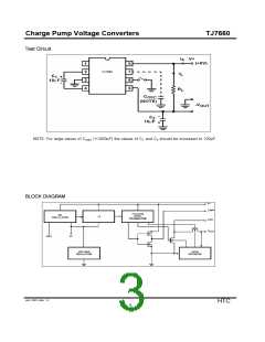
Charge Pump Voltage Converters
TJ7660
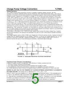
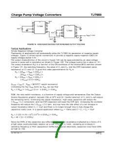
It is also possible to increase the conversion efficiency of the TJ7660 at low load levels by lowering
the oscillator frequency. This reduces the switching losses, and is shown in Figure 18. However,
lowering the oscillator frequency will cause an undesirable increase in the impedance of the pump
(C1) and reservoir (C2) capacitors; this is overcome by increasing the values of C1 and C2 by the
same factor that the frequency has been reduced. For example, the addition of a 100pF capacitor
between pin 7(OSC) and V+ will lower the oscillator frequency to 1kHz from its nominal frequency
of 10kHz (a multiple of 10), and thereby necessitate a corresponding increase in the value of C1
and C2(from 10µF to 100µF).
TJ7660
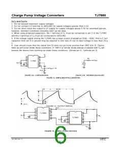
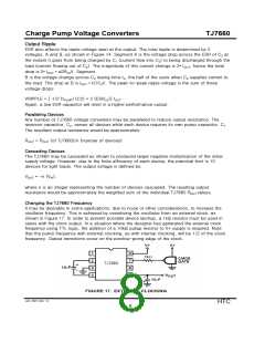
Positive Voltage Doubling
The TJ7660 may be employed to achieve positive voltage doubling using the circuit shown in
Figure19. In this application, the pump inverter switches of the TJ7660 are used to charge C1 to a
voltage level of V+ -VF (where V+ is the supply voltage and VF is the forward voltage drop of
diode D1). On the transfer cycle, the voltage on C1 plus the supply voltage (V+) is applied through
diode D2 to capacitor C2. The voltage thus created on C2 becomes (2V+) - (2VF) or twice the
supply voltage minus the combined forward voltage drops of diodes D1 and D2.
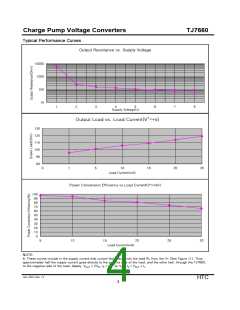
The source impedance of the output (VOUT) will depend on the output current, but for V+ = 5V and
an output current of 10mA it will be approximately 60Ω.
TJ7660
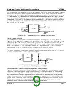
Combined Negative Voltage Conversion and Positive Supply Doubling
Figure 20 combines the functions shown in Figures 13 and Figure 19 to provide negative voltage
conversion and positive voltage doubling simultaneously. This approach would be, for example,
suitable for generating +9V and -5V from an existing +5V supply. In this instance capacitors C1
and C3 perform the pump and reservoir functions respectively for the generation of the negative
voltage, while capacitors C2 and C4 are pump and reservoir respectively for the doubled positive
voltage. There is a penalty in this configuration which combines both functions, however, in that
the source impedances of the generated supplies will be somewhat higher due to the finite
impedance of the common charge pump driver at pin 2 of the device.
Jan. 2007-Rev 1.0
HTC
9

 HTC [ HTC KOREA TAEJIN TECHNOLOGY CO. ]