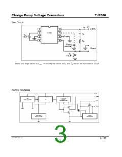
Charge Pump Voltage Converters
TJ7660
TJ7660
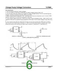
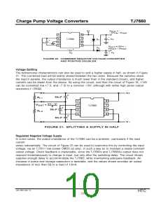
Voltage Splitting
The bidirectional characteristics can also be used to split a higher supply in half, as shown in Figure
21. The combined load will be evenly shared between the two sides. Because the switches share
the load in parallel, the output impedance is much lower than in the standard circuits, and higher
currents can be drawn from the device. By using this circuit, and then the circuit of Figure 16, +15V
can be converted (via +7.5, and -7.5) to a nominal -15V, although with rather high series output
resistance (~250Ω).
TJ7660
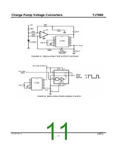
Regulated Negative Voltage Supply
In some cases, the output impedance of the TJ7660 can be a problem, particularly if the load
current
varies substantially. The circuit of Figure 22 can be used to overcome this by controlling the input
voltage, via an TJ7611 low-power CMOS op amp, in such a way as to maintain a nearly constant
output voltage. Direct feedback is inadvisable, since the TJ7660s and TJ7660As output does not
respond instantaneously to change in input, but only after the switching delay. The circuit shown
supplies enough delay to accommodate the TJ7660, while maintaining adequate feedback. An
increase in pump and storage capacitors is desirable, and the values shown provides an output
impedance of less than 5Ω to a load of 10mA.
Jan. 2007-Rev 1.0
HTC
10

 HTC [ HTC KOREA TAEJIN TECHNOLOGY CO. ]