Charge Pump Voltage Converters
TJ7660
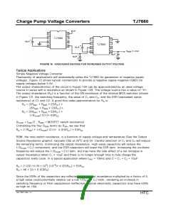
Output Ripple
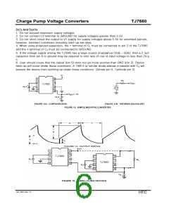
ESR also affects the ripple voltage seen at the output. The total ripple is determined by 2
voltages, A and B, as shown in Figure 14. Segment A is the voltage drop across the ESR of C2 at
the instant it goes from being charged by C1 (current flow into C2) to being discharged through the
load (current flowing out of C2). The magnitude of this current change is 2• IOUT, hence the total
drop is 2• IOUT • eSRC2V. Segment
B is the voltage change across C2 during time t2, the half of the cycle when C2 supplies current to
the load. The drop at B is lOUT • t2/C2V. The peak-to-peak ripple voltage is the sum of these
voltage drops:
VRIPPLE = [ 1/2 (fPUMP) (C2) + 2 (ESRC2)] IOUT
Again, a low ESR capacitor will reset in a higher performance output.
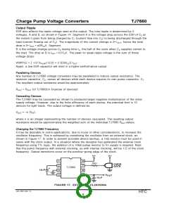
Paralleling Devices
Any number of TJ7660 voltage converters may be paralleled to reduce output resistance. The
reservoir capacitor, C2, serves all devices while each device requires its own pump capacitor, C1.
The resultant output resistance would be approximately:
R
OUT = ROUT (of TJ7660)/n (number of devices)
Cascading Devices
The TJ7660 may be cascaded as shown to produced larger negative multiplication of the initial
supply voltage. However, due to the finite efficiency of each device, the practical limit is 10
devices for light loads. The output voltage is defined by:
VOUT = -n (VIN),
where n is an integer representing the number of devices cascaded. The resulting output
resistance would be approximately the weighted sum of the individual TJ7660 ROUT values.
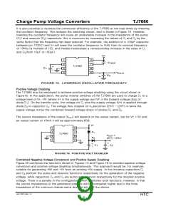
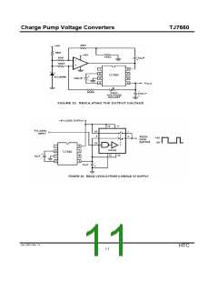
Changing the TJ7660 Frequency
It may be desirable in some applications, due to noise or other considerations, to increase the
oscillator frequency. This is achieved by overdriving the oscillator from an external clock, as
shown in Figure 17. In order to prevent possible device latchup, a 1kΩ resistor must be used in
series with the clock output. In a situation where the designer has generated the external clock
frequency using TTL logic, the addition of a 10kΩ pullup resistor to V+ supply is required. Note
that the pump frequency with external clocking, as with internal clocking, will be 1/2 of the clock
frequency. Output transitions occur on the positive-going edge of the clock.
TJ7660
Jan. 2007-Rev 1.0
HTC
8

 HTC [ HTC KOREA TAEJIN TECHNOLOGY CO. ]