Charge Pump Voltage Converters
TJ7660
Absolute Maximum Ratings
Supply Voltage TJ7660
+10.5V
V
V
-0.3V to [(V+ +0.3V) for V+] < 5.5V
(V+ -5.5V) to [(V+ +0.3V) for V+] > 5.5V
20µA for V+ > 3.5V
LV and OSC Input Voltage (Note2)
Current into LV (Note 2)
Output Short Duration (VSUPPLY ≤ 5.5V)
Operating Ambient Temperature
uA
Continuous
0℃ to 70℃
℃
Thermal Information
Thermal Resistance (Typical, Note 1)
PDIP Package
θJC (℃/W)
N/A
θJA (℃/W)
150
SOIC Package
165
N/A
Metal Can Package (TJ7660 Only)
Maximum Storage Temperature Range
160
70
-65oC to 150℃
Maximum Lead Temperature (Soldering, 10s)
(SOIC - Lead Tips Only)
300℃
CAUTION: Stresses above those listed in “Absolute Maximum Ratings” may cause permanent damage to the device. This is
a stress only rating and operation of the device at these or any other conditions above those indicated in the operational
sections of this specification is not implied.
ELECTRICAL CHARACTERISTIC (TJ7660, V+ = 5V, TA = 25oC, COSC = 0, unless Otherwise Specified
TJ7660
UNITS
PARAMETER
Supply Current
SYMBOL
TEST CONDITIONS
RL = ∞
MIN
-
TYP MAX
µA
V
I+
100
-
180
3.5
-
VL+
MIN ≤ TA ≤ MAX, RL =10kΩ, LV to GND
MIN ≤ TA ≤ MAX, RL =10kΩ,LVto Open
IOUT =20mA, TA =25℃
Supply Voltage Range -Lo
2.0
3
VH+
V
Supply Voltage Range -Hi
Output Source Resistance
-
ROUT
Ω
-
60
-
100
IOUT =20mA, -40℃ ≤ TA ≤ 85℃
V+ = 2V, IOUT = 3mA, LV to GND
0℃≤ TA ≤ 70℃
Ω
Ω
-
-
-
300
-
V+ = 2V, IOUT = 3mA, LV to GND,
-55℃ ≤ TA ≤ 125℃
-
-
400
Ω
fOSC
PEF
kHz
%
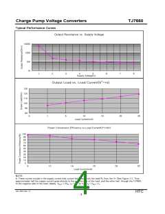
Oscillator Frequency
Power Efficiency
Voltage Conversion Efficie
NOTES
-
95
98
10
98
-
-
-
RL =5kΩ
RL = ∞
VOUT EF
%
99.9
1. θJA is measured with the component mounted on an evaluation PC board in free air.
2. Connecting any input terminal to voltages greater than V+ or less than GND may cause
destructive latchup. It is recommended that no inputs from sources operating from
external supplies be applied prior to “power up” of the TJ7660.
Jan. 2007-Rev 1.0
HTC
2

 HTC [ HTC KOREA TAEJIN TECHNOLOGY CO. ]