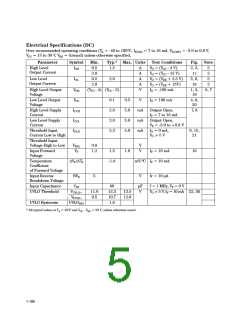
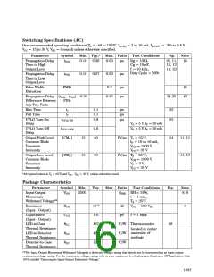
Switching Specifications (AC)
Over recommended operating conditions (TA = -40 to 100°C, IF(ON) = 7 to 16 mA, VF(OFF) = -3.0 to 0.8 V,
VCC = 15 to 30 V, VEE = Ground) unless otherwise specified.
Parameter
Symbol
Min. Typ.* Max. Units
Test Conditions
Fig.
Note
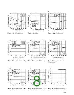
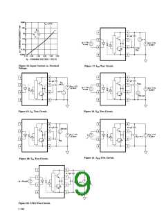
Propagation Delay
Time to High
Output Level
tPLH
0.10
0.30
0.50
µs
Rg = 10 Ω,
Cg = 10 nF,
f = 10 kHz,
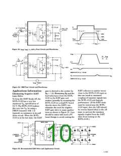
10, 11,
12, 13
14, 23
14
Duty Cycle = 50%
Propagation Delay
Time to Low
tPHL
0.10
0.27
0.50
µs
Output Level
Pulse Width
Distortion
Propagation Delay (tPHL - tPLH) -0.35
PWD
0.3
µs
µs
15
10
0.35
34,35
Difference Between
Any Two Parts
PDD
Rise Time
Fall Time
UVLO Turn On
Delay
UVLO Turn Off
Delay
Output High Level
Common Mode
Transient
tr
tf
0.1
0.1
0.8
µs
µs
µs
23
22
tUVLO ON
VO > 5 V, IF = 10 mA
VO < 5 V, IF = 10 mA
tUVLO OFF
|CMH|
0.6
30
15
15
kV/µs TA = 25°C,
IF = 10 to 16 mA,
24
11, 12
11, 13
VCM = 1500 V,
VCC = 30 V
Immunity
Output Low Level
Common Mode
Transient
|CML|
30
kV/µs TA = 25°C,
VCM = 1500 V,
VF = 0 V,
Immunity
VCC = 30 V
*All typical values at TA = 25°C and VCC - VEE = 30 V, unless otherwise noted.
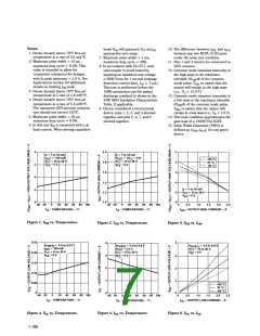
Package Characteristics
Parameter
Symbol
Min.
Typ.
Max. Units
Test Conditions
Fig.
Note
Input-Output
V
ISO
2500
VRMS RH < 50%,
8, 9
Momentary
t = 1 min.,
Withstand Voltage**
Resistance
(Input - Output)
Capacitance
(Input - Output)
LED-to-Case
Thermal Resistance
LED-to-Detector
TA = 25°C
RI-O
CI-O
θLC
θLD
θDC
1012
0.6
Ω
VI-O = 500 VDC
9
pF
f = 1 MHz
467
442
126
°C/W Thermocoupler
28
located at center
underside of
package
°C/W
°C/W
Thermal Resistance
Detector-to-Case
Thermal Resistance
**The Input-Output Momentary Withstand Voltage is a dielectric voltage rating that should not be interpreted as an input-output
continuous voltage rating. For the continuous voltage rating refer to your equipment level safety specification or HP Application Note
1074 entitled “Optocoupler Input-Output Endurance Voltage.”
1-187

 HP [ HEWLETT-PACKARD ]