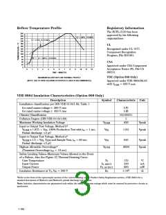
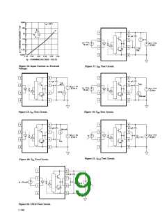
Reflow Temperature Profile
Regulatory Information
The HCPL-3120 has been
approved by the following
organizations:
260
240
220
∆T = 145°C, 1°C/SEC
∆T = 115°C, 0.3°C/SEC
200
180
160
140
120
100
UL
Recognized under UL 1577,
Component Recognition
Program, File E55361.
80
∆T = 100°C, 1.5°C/SEC
60
40
20
0
CSA
Approved under CSA Component
Acceptance Notice #5, File CA
88324.
0
1
2
3
4
5
6
7
8
9
10
11
12
TIME – MINUTES
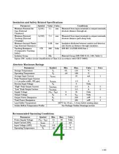
VDE (Option 060 Only)
MAXIMUM SOLDER REFLOW THERMAL PROFILE
(NOTE: USE OF NON-CHLORINE ACTIVATED FLUXES IS RECOMMENDED.)
Approved under VDE 0884/06.92
with VIORM = 630 V peak.
VDE 0884 Insulation Characteristics (Option 060 Only)
Description
Symbol
Characteristic Unit
Installation classification per DIN VDE 0110/1.89, Table 1
for rated mains voltage ≤ 300 V rms
for rated mains voltage ≤ 450 V rms
I-IV
I-III
Climatic Classification
Pollution Degree (DIN VDE 0110/1.89)
55/100/21
2
Maximum Working Insulation Voltage
Input to Output Test Voltage, Method b*
V
630
Vpeak
Vpeak
IORM
V
IORM
x 1.875 = V , 100% Production Test with t = 1 sec,
V
PR
1181
PR
m
Partial discharge <5 pC
Input to Output Test Voltage, Method a*
V
x 1.5 = V , Type and Sample Test, t = 60 sec,
V
PR
945
Vpeak
Vpeak
IORM
PR
m
Partial discharge <5 pC
Highest Allowable Overvoltage*
V
IOTM
6000
(Transient Overvoltage t = 10 sec)
ini
Safety Limiting Values–Maximum Values Allowed in the Event
of a Failure, Also See Figure 37, Thermal Derating Curve.
Case Temperature
Input Current
Output Power
T
175
230
600
°C
mA
mW
S
I
P
S, INPUT
S, OUTPUT
9
Insulation Resistance at T , V = 500 V
R
S
≥ 10
Ω
S
IO
*Refer to the front of the optocoupler section of the current catalog, under Product Safety Regulations section, (VDE 0884) for a
detailed description of Method a and Method b partial discharge test profiles.
Note: Isolation characteristics are guaranteed only within the safety maximum ratings which must be ensured by protective circuits in
application.
1-184

 HP [ HEWLETT-PACKARD ]