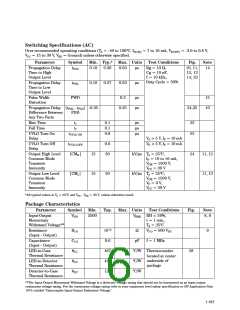
1
2
3
4
8
7
6
5
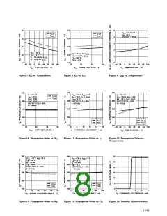
I
0.1 µF
F
I
= 7 to 16 mA
F
V
= 15
CC
to 30 V
+
–
t
t
f
r
500 Ω
+
V
O
–
90%
10 KHz
50% DUTY
CYCLE
10 Ω
10 nF
50%
10%
V
OUT
t
t
PHL
PLH
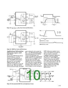
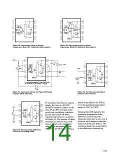
Figure 23. tPLH, tPHL, tr, and tf Test Circuit and Waveforms.
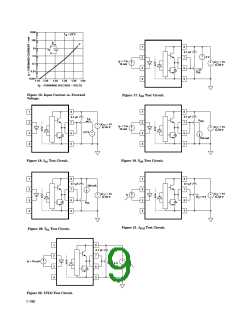
V
CM
δV
δt
V
CM
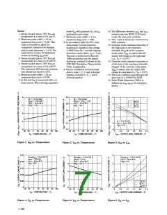
1
2
3
4
8
7
6
5
=
∆t
I
F
0.1 µF
A
B
0 V
∆t
+
–
+
–
V
O
5 V
V
= 30 V
CC
V
V
OH
V
O
SWITCH AT A: I = 10 mA
F
V
O
OL
SWITCH AT B: I = 0 mA
F
+
V
= 1500 V
CM
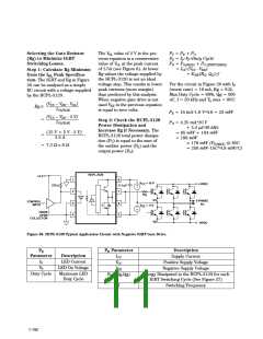
Figure 24. CMR Test Circuit and Waveforms.
IGBT collector or emitter traces
close to the HCPL-3120 input as
this can result in unwanted
coupling of transient signals into
the HCPL-3120 and degrade
performance. (If the IGBT drain
must be routed near the HCPL-
3120 input, then the LED should
be reverse-biased when in the off
state, to prevent the transient
signals coupled from the IGBT
drain from turning on the
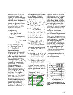
Applications Information
Eliminating Negative IGBT
Gate Drive
To keep the IGBT firmly off, the
HCPL-3120 has a very low
maximum VOL specification of
0.5 V. The HCPL-3120 realizes
this very low VOL by using a
DMOS transistor with 1 Ω
gate is shorted to the emitter by
Rg + 1 Ω. Minimizing Rg and the
lead inductance from the HCPL-
3120 to the IGBT gate and
emitter (possibly by mounting the
HCPL-3120 on a small PC board
directly above the IGBT) can
eliminate the need for negative
IGBT gate drive in many applica-
tions as shown in Figure 25. Care
should be taken with such a PC
board design to avoid routing the
(typical) on resistance in its pull
down circuit. When the HCPL-
3120 is in the low state, the IGBT
HCPL-3120.)
HCPL-3120
+5 V
1
2
3
4
8
V
= 18 V
CC
+ HVDC
270 Ω
0.1 µF
+
–
7
Rg
Q1
3-PHASE
AC
CONTROL
INPUT
6
5
74XXX
OPEN
COLLECTOR
Q2
- HVDC
Figure 25. Recommended LED Drive and Application Circuit.
1-191

 HP [ HEWLETT-PACKARD ]