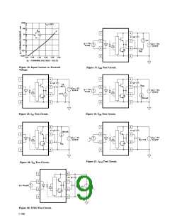
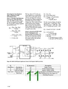
θ
= 442 °C/W
LD
TJE = LED junction temperature
TJD = detector IC junction temperature
T
T
JD
JE
TC = case temperature measured at the center of the package bottom
θLC = LED-to-case thermal resistance
θLD = LED-to-detector thermal resistance
θ
= 467 °C/W
θ
= 126 °C/W
DC
LC
T
C
θDC = detector-to-case thermal resistance
θ
= 83 °C/W*
CA
θCA = case-to-ambient thermal resistance
θCA will depend on the board design and the placement of the part.
T
A
Figure 28. Thermal Model.
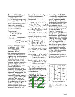
CMR with the LED On
(CMRH).
A high CMR LED drive circuit
must keep the LED on during
common mode transients. This is
achieved by overdriving the LED
current beyond the input
threshold so that it is not pulled
below the threshold during a
transient. A minimum LED cur-
rent of 10 mA provides adequate
margin over the maximum IFLH of
5 mA to achieve 15 kV/µs CMR.
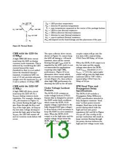
The open collector drive circuit,
shown in Figure 32, cannot keep
the LED off during a +dVcm/dt
transient, since all the current
flowing through CLEDN must be
supplied by the LED, and it is not
recommended for applications
requiring ultra high CMRL
performance. Figure 33 is an
alternative drive circuit which,
like the recommended application
circuit (Figure 25), does achieve
ultra high CMR performance by
shunting the LED in the off state.
coupler output will go into the
low state with a typical delay,
UVLO Turn Off Delay, of 0.6 µs.
When the HCPL-3120 output is in
the low state and the supply
voltage rises above the HCPL-
3120 VUVLO+ threshold (11.0 <
VUVLO+ < 13.5) the optocoupler
output will go into the high state
(assumes LED is “ON”) with a
typical delay, UVLO Turn On
Delay of 0.8 µs.
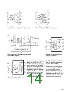
CMR with the LED Off
(CMRL).
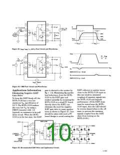
IPM Dead Time and
Propagation Delay
Specifications.
Under Voltage Lockout
Feature.
The HCPL-3120 contains an
A high CMR LED drive circuit
must keep the LED off (VF ≤
VF(OFF)) during common mode
transients. For example, during a
-dVcm/dt transient in Figure 31,
the current flowing through CLEDP
also flows through the RSAT and
VSAT of the logic gate. As long as
the low state voltage developed
across the logic gate is less than
VF(OFF), the LED will remain off
and no common mode failure will
occur.
The HCPL-3120 includes a
under voltage lockout (UVLO)
feature that is designed to protect
the IGBT under fault conditions
which cause the HCPL-3120
supply voltage (equivalent to the
fully-charged IGBT gate voltage)
to drop below a level necessary to
keep the IGBT in a low resistance
state. When the HCPL-3120
output is in the high state and the
supply voltage drops below the
HCPL-3120 VUVLO– threshold
(9.5 < VUVLO– < 12.0) the opto-
Propagation Delay Difference
(PDD) specification intended to
help designers minimize “dead
time” in their power inverter
designs. Dead time is the time
period during which both the
high and low side power
transistors (Q1 and Q2 in Figure
25) are off. Any overlap in Q1
and Q2 conduction will result in
large currents flowing through
the power devices between the
high and low voltage motor rails.
1-194

 HP [ HEWLETT-PACKARD ]