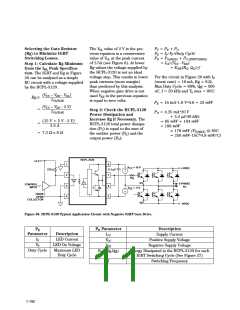
C
1
2
3
4
8
7
6
5
1
2
3
4
8
7
6
5
LEDO1
C
C
C
C
LEDP
LEDP
C
LEDO2
LEDN
LEDN
SHIELD
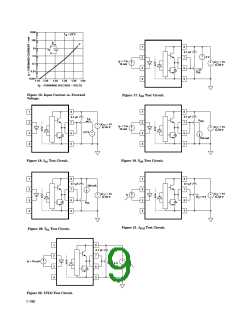
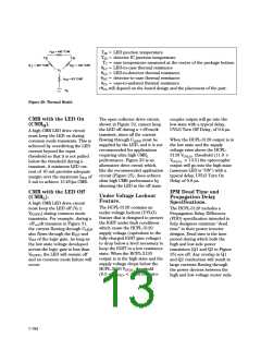
Figure 29. Optocoupler Input to Output
Capacitance Model for Unshielded Optocouplers.
Figure 30. Optocoupler Input to Output
Capacitance Model for Shielded Optocouplers.
+5 V
1
2
3
4
8
7
6
5
0.1
µF
+
–
C
I
LEDP
V
= 18 V
CC
+
1
2
3
4
8
7
6
5
LEDP
V
SAT
+5 V
–
C
LEDP
• • •
• • •
C
LEDN
Rg
SHIELD
C
I
LEDN
Q1
LEDN
* THE ARROWS INDICATE THE DIRECTION
OF CURRENT FLOW DURING –dV /dt.
SHIELD
CM
+
–
V
CM
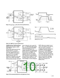
Figure 31. Equivalent Circuit for Figure 25 During
Common Mode Transient.
Figure 32. Not Recommended Open
Collector Drive Circuit.
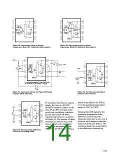
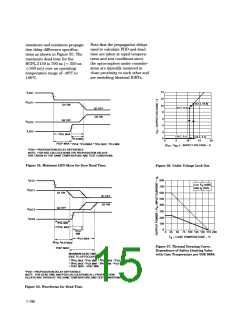
which is specified to be 350 ns
over the operating temperature
range of -40°C to 100°C.
To minimize dead time in a given
design, the turn on of LED2
should be delayed (relative to the
turn off of LED1) so that under
worst-case conditions, transistor
Q1 has just turned off when
transistor Q2 turns on, as shown
in Figure 34. The amount of delay
necessary to achieve this condi-
tions is equal to the maximum
value of the propagation delay
1
2
3
4
8
7
6
5
+5 V
C
C
LEDP
Delaying the LED signal by the
maximum propagation delay
difference ensures that the
minimum dead time is zero, but it
does not tell a designer what the
maximum dead time will be. The
maximum dead time is equivalent
to the difference between the
LEDN
SHIELD
difference specification, PDDMAX
,
Figure 33. Recommended LED Drive
Circuit for Ultra-High CMR.
1-195

 HP [ HEWLETT-PACKARD ]