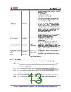
RFM70 V1.0
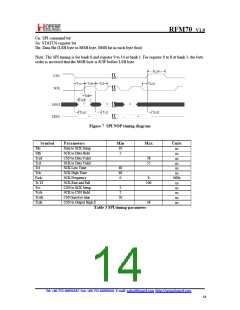
Cn: SPI command bit
Sn: STATUS register bit
Dn: Data Bit (LSB byte to MSB byte, MSB bit in each byte first)
Note: The SPI timing is for bank 0 and register 9 to 14 at bank 1. For register 0 to 8 at bank 1, the byte
order is inversed that the MSB byte is R/W before LSB byte.
Figure 7 SPI NOP timing diagram
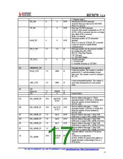
Symbol
Tdc
Parameters
Min
10
Max
Units
ns
ns
Data to SCK Setup
SCK to Data Hold
CSN to Data Valid
SCK to Data Valid
SCK Low Time
Tdh
2
Tcsd
Tcd
38
55
ns
ns
Tcl
40
40
0
ns
Tch
SCK High Time
ns
MHz
Fsck
Tr,Tf
Tcc
SCK Frequency
8
SCK Rise and Fall
CSN to SCK Setup
SCK to CSN Hold
CSN Inactive time
CSN to Output High Z
100
ns
ns
ns
ns
ns
2
2
Tcch
Tcwh
Tcdz
50
38
Table 3 SPI timing parameter
Tel: +86‐755‐86096587 Fax: +86‐755‐86096602 E‐mail: sales@hoperf.com http://www.hoperf.com
14

 HOPERF [ HOPERF ]